10
ICM7228
8WRITE Input Data Input Will Be Written to Control Register or Display RAM on Rising Edge of WRITE.
9 MODE Input Selects Data to Be Loaded to Control Register or Display RAM: High, Loads Control Register;
Low, Loads Display RAM.
10 ID4,
(SHUTDOWN
)
Input When “MODE” Low: Display Data Input, Bit 5.
When “MODE” High: Control Bit, Low Power Mode Select: High, Normal Operation; Low,
Oscillator and Display Disabled.
11 ID1 Input When “MODE” Low: Display Data Input, Bit 2.
When “MODE” High and “ID7 (DATA COMING)” Low: Digit Address, Bit 2, Single Digit Update
Mode.
12 ID0 Input When “MODE” Low: Display Data Input, Bit 1.
When “MODE” High and “ID7 (DATA COMING)” Low: Digit Address, LSB, Single Digit Update
Mode.
13 ID2 Input When “MODE” Low: Display Data Input, Bit 3.
When “MODE” High and “ID7 (DATA COMING)” Low: Digit Address, MSB, Single Digit Update
Mode.
14 ID3 Input When “MODE” Low: Display Data Input, Bit 4.
When “MODE” High: RAM Bank Select (Decode Modes Only): High, RAM Bank A; Low, RAM
Bank B.
15 DP Output LED Display Decimal Point and Segments a, b, and d Drive Lines
16 SEG a
17 SEG b
18 SEG d
19 V
DD
Supply Device Positive Power Supply Rail.
20 SEG c Output LED Display Segments c, e, f and g Drive Lines.
21 SEG e
22 SEG f
23 SEG g
24 DIGIT 8 Output LED Display Digits 8, 2, 5 and 7 Drive Lines.
25 DIGIT 2
26 DIGIT 5
27 DIGIT 7
28 V
SS
Supply Device Ground or Negative Power Supply Rail.
TABLE 3. ICM7228C PIN ASSIGNMENTS AND DESCRIPTIONS
PIN NO. NAME FUNCTION DESCRIPTION
1 SEG c Output LED Display Segments c, e, band Decimal Point Drive Lines.
2 SEG e
3 SEG b
4DP
5 DA0 Input Digit Address Input, Bit 1 LSB.
6 DA1 Input Digit Address Input, Bit 2.
7ID7,
(INPUT DP
)
Input Display Decimal Point Data Input, Negative True.
8WRITE
Input Data Input Will Be Written to Display RAM on Rising Edge of WRITE.
TABLE 2. ICM7228B PIN ASSIGNMENTS AND DESCRIPTIONS (Continued)
PIN NO. NAME FUNCTION DESCRIPTION
11
ICM7228
Detailed Description
System Interfacing and Data Entry Modes,
ICM7228A and ICM7228B
The ICM7228A/B devices are compatible with the
architectures of most microprocessor systems. Their fast
switching characteristics makes it possible to access them as
a memory mapped I/O device with no wait state necessary in
most microcontroller systems. All the ICM7228A/B inputs,
including MODE, feature a 250ns minimum setup and 0ns
hold time with a 200ns minimum WRITE
pulse. Input logic
levels are TTL and CMOS compatible. Figure 9 shows a
generic method of driving the ICM7228A/B from a
microprocessor bus. To the microprocessor, each device
appears to be 2 separate I/O locations; the Control Register
and the Display RAM. Selection between the two is
accomplished by the MODE input driven by address line A0.
Input data is placed on the lD0 - lD7 lines. The WRITE
input
acts as both a device select and write cycle timing pulse. See
Figure 1 and Switching Specifications Table for write cycle
timing parameters.
The ICM7228A/B have three data entry modes: Control
Register update without RAM update, sequential 8-digit
update and single digit update. In all three modes a control
word is first written by pulsing the WRITE input while the
MODE input is high, thereby latching data into the Control
Register. The logic level of individual bits in the Control
Register select Shutdown, Decode/No Decode, Hex/Code B,
RAM bank A/B and Display RAM digit address as shown in
Tables 1 and 2.
The ICM7228A/B Display RAM is divided into 2 banks, called
bank A and B. When using the Hexadecimal or code B display
modes, these RAM banks can be selected separately. This
allows two separate sets of display data to be stored and
displayed alternately. Notice that the RAM bank selection is not
possible in No-Decode mode, this is because the display data
in the No-Decode mode has 8 bits, but in Decoded schemes
(Hex/Code B) is only 4 bits (lD0 - lD3 data). It should also be
mentioned that the decimal point is independent of selected
bank, a turned on decimal point will remain on for either bank.
Selection of the RAM banks is controlled by lD3 input. The lD3
logic level (during Control Register update) selects which bank
of the internal RAM to be written to and/or displayed.
Control Register Update without RAM Update
The Control Register can be updated without changing the
display data by a single pulse on the WRITE input, with MODE
high and DATA COMING low. If the display is being decoded
(Hex/Code B), then the value of lD3 determines which RAM
bank will be selected and displayed for all eight digits.
9 HEXA/CODE
B/SHUTDOWN
Input Three Level Input. Display Function Control: High, Hexadecimal Decoding; Float, Code B
Decoding; Low, Oscillator, and Display Disabled.
10 DA2 Input Digit Address Input, Bit 3, MSB.
11 ID1 Input Display Data Inputs.
12 ID0
13 ID2
14 ID3
15 DIGIT 1 Output LED Display Digits 1, 2, 5 and 8 Drive Lines.
16 DlGlT 2
17 DIGIT 5
18 DlGlT 8
19 V
DD
Supply Device Positive Power Supply Rail.
20 DIGIT 4 Output LED Display Digits 4, 7, 6 and 3 Drive Lines.
21 DlGlT 7
22 DlGlT 6
23 DIGlT 3
24 SEG f Output LED Display Segments f, d, g and a Drive Lines.
25 SEG d
26 SEG g
27 SEG a
28 V
SS
Supply Device Ground or Negative Power Supply Rail.
TABLE 3. ICM7228C PIN ASSIGNMENTS AND DESCRIPTIONS (Continued)
PIN NO. NAME FUNCTION DESCRIPTION
12
ICM7228
Sequential 8-Digit Update
The logic state of DATA COMING (lD7) is also latched during
a Control Register update. If the latched value of DATA
COMING (lD7) is high, the display becomes blanked and a
sequential 8-digit update is initiated. Display data can now
be written into RAM with 8 successive WRITE pulses,
starting with digit 1 and ending with digit 8 (See Figure 2).
After all 8 RAM locations have been written to, the display
turns on again and the new data is displayed. Additional
write pulses are ignored until a new Control Register update
is performed. All 8 digits are displayed in the format
(Hex/Code B or No Decode) specified by the control word
that preceded the 8 digit update. If a decoding scheme
(Hex/Code B) is to be used, the value of lD3 during the
control word update determines which RAM bank will be
written to.
Single Digit Update
In this mode each digit data in the display RAM can be updated
individually without changing the other display data. First, with
MODE input high, a control word is written to the Control
Register carrying the following information; DATA COMING
(lD7) low, the desired display format data on lD4 - lD6, the RAM
bank selected by lD3 (if decoding is selected) and the address
of the digit to be updated on data lines lD0 - lD2 (See Table 4).
A second write to the ICM7228A/B, this time with MODE input
low, transfers the data at the lD0 - lD7 inputs into the selected
digit’s RAM location. In single digit update mode, each
individual digit’s data can be specified independently for being
displayed in Decoded or No-Decode mode. For those digits
which decoding scheme (Hex/Code B) is selected, only one
can be effective at a time. Whenever a control word is written,
the specified decoding scheme will be applied to all those digits
which selected to be displayed in Decoded mode.
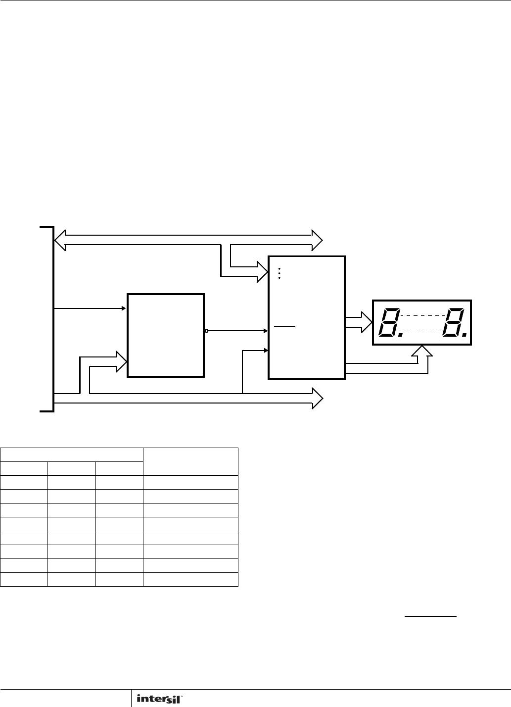
System Interfacing, ICM7228C
The ICM7228C is directly compatible with the architecture of
most microprocessor systems. Its fast switching
characteristics make it possible to access them as a memory
mapped I/O device with no wait state necessary in most
microcontroller systems. All the ICM7228C inputs, excluding
HEXA/CODE B/SHUTDOWN, feature a 250ns minimum
setup and 0ns hold time with a 200ns minimum WRITE pulse.
Input logic levels are TTL and CMOS compatible. Figure 10
shows a generic method of driving the ICM7228C from a
microprocessor bus. To the microprocessor, the 8 bytes of the
Display RAM appear to be 8 separate I/O locations. Loading
the ICM7228C is quite similar to a standard memory write
cycle. The address of the digit to be updated is placed on lines
DA0 - DA2, the data to be written is placed on lines ID0 - lD3
and ID7, then a low pulse on WRITE input will transfer the
data in. See Figure 3 and Switching Characteristics Table for
write cycle timing parameters.
The ICM7228C does not have any control register, and also
does not provide the No Decode display format. Hexadecimal
or Code B character selection and shutdown mode are directly
controlled through the three level input at Pin 9, which is
accordingly called HEXA/CODE B/SHUTDOWN
. See Table 3
for input and output definitions of the ICM7228C.
I/O OR
MEMORY
WRITE PULSE
DECODER
ENABLE
ADDRESS
DECODER
ID0
ID7
INTERSIL
ICM7228A/B
SEGMENTS
DRIVE
WRITE
MODE
DIGITS
DRIVE
A0
DEVICE SELECT
AND
WRITE PULSE
LED DISPLAY
ADDRESS BUS A0 - A15
A1-A15
DATA BUS D0-D7
D0 - D7
MICROPROCESSOR SYSTEM
FIGURE 9. ICM7228A/B MICROPROCESSOR SYSTEM INTERFACING
TABLE 4. DIGITS ADDRESS, ICM7228A/B
INPUT DATA LINES
SELECTED DIGIT1D2 lD2 lD0
0 0 0 DlGlT 1
0 0 1 DlGlT 2
0 1 0 DIGlT 3
0 1 1 DlGlT 4
1 0 0 DIGIT 5
1 0 1 DlGlT 6
1 1 0 DlGlT 7
1 1 1 DlGlT 8

ICM7228BIBIZ

Mfr. #:
Manufacturer:
Renesas / Intersil
Description:
LED Display Drivers DISPLAY 8 DIG LED 07228B DRVR 28W IND
Lifecycle:
New from this manufacturer.
Delivery:
DHL FedEx Ups TNT EMS
Payment:
T/T Paypal Visa MoneyGram Western Union