XCR3512XL-12PQG208I

XCR3512XL: 512 Macrocell CPLD
4 www.xilinx.com DS081 (v2.0) March 31, 2006
Product Specification
R
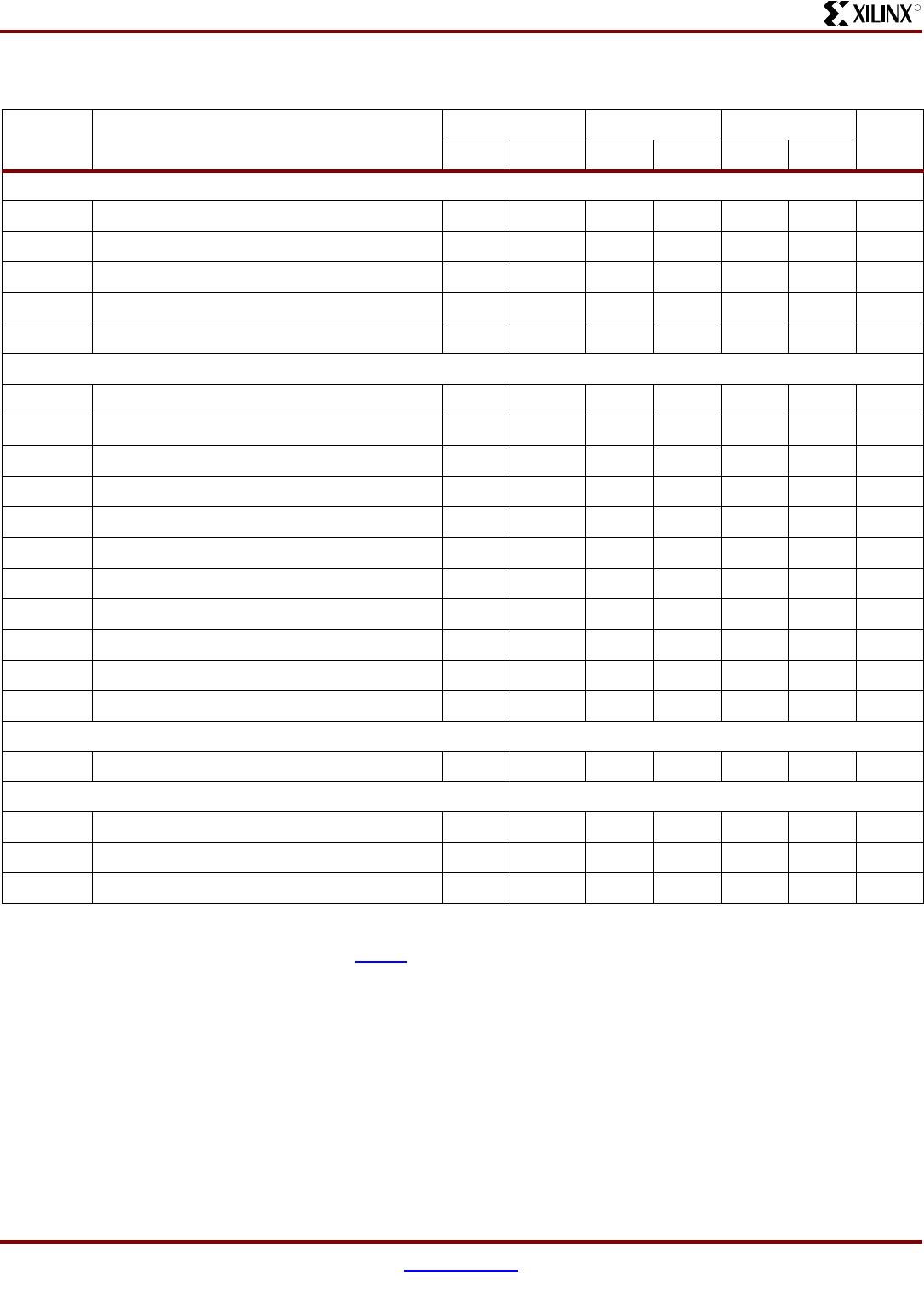
Internal Timing Parameters
(1,2)
Symbol Parameter
-7 -10 -12
UnitMin. Max. Min. Max. Min. Max.
Buffer Delays
T
IN
Input buffer delay - 2.5 - 3.3 - 4.0 ns
T
FIN
Fast input buffer delay - 4.7 - 4.3 - 4.3 ns
T
GCK
Global clock buffer delay - 1.5 - 1.3 - 1.5 ns
T
OUT
Output buffer delay - 2.5 - 3.2 - 3.8 ns
T
EN
Output buffer enable/disable delay - 4.5 - 5.2 - 6.0 ns
Internal Register and Combinatorial Delays
T
LDI
Latch transparent delay - 1.3 - 1.6 - 2.0 ns
T
SUI
Register setup time 0.8 - 1.0 - 1.2 - ns
T
HI
Register hold time 0.3 - 0.5 - 0.7 - ns
T
ECSU
Register clock enable setup time 2.0 - 2.5 - 3.0 - ns
T
ECHO
Register clock enable hold time 3.0 - 4.5 - 5.5 - ns
T
COI
Register clock to output delay - 1.0 - 1.3 - 1.6 ns
T
AOI
Register async. S/R to output delay - 2.0 - 2.0 - 2.2 ns
T
RAI
Register async. recovery - 5.0 - 7.0 - 8.0 ns
T
PTCK
Product term clock delay - 2.5 - 2.5 - 3.0 ns
T
LOGI1
Internal logic delay (single p-term) - 2.0 - 2.5 - 3.0 ns
T
LOGI2
Internal logic delay (PLA OR term) - 2.5 - 3.5 - 4.2 ns
Feedback Delays
T
F
ZIA delay - 3.1 - 4.5 - 6.0 ns
Time Adders
T
LOGI3
Fold-back NAND delay - 2.0 - 2.5 - 3.0 ns
T
UDA
Universal delay - 3.5 - 4.0 - 4.0 ns
T
SLEW
Slew rate limited delay - 5.0 - 5.0 - 6.0 ns
Notes:
1. These parameters guaranteed by design and/or characterization, not testing.
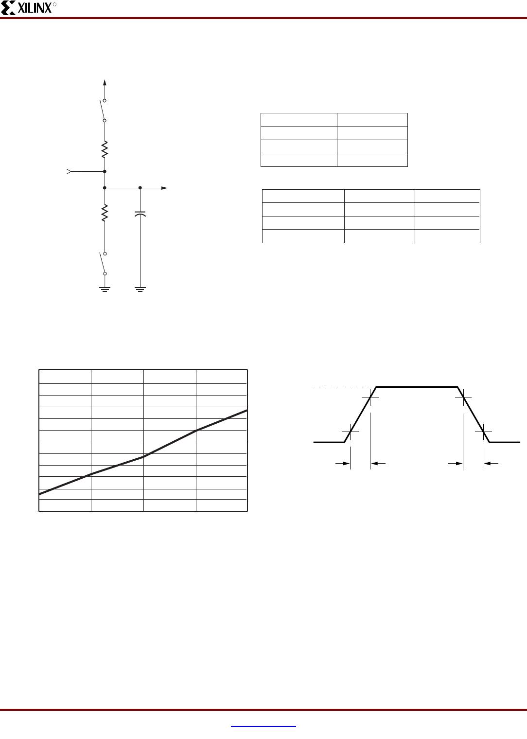
2. See the CoolRunner XPLA3 family data sheet (
DS012) for timing model.
XCR3512XL: 512 Macrocell CPLD
DS081 (v2.0) March 31, 2006 www.xilinx.com 5
Product Specification
R
Switching Characteristics
Figure 3: AC Load Circuit
DS023_03_102401
Component Values
R1 390Ω
R2 390Ω
C1 35 pF
Measurement S1 S2
T
POE
(High)
T
POE
(Low)
T
P
Open Closed
Closed Open
Closed
Closed
V
CC
V
OUT
V
IN
C1
R1
R2
S1
S2
Note: For T
POD
, C1 = 5 pF. Delay measured at
output level of V
OL
+ 300 mV, V
OH
– 300 mV.
Figure 4: Derating Curve for T
PD2
6.3
6.4
6.5
6.6
6.7
6.8
6.9
7.0
7.1
7.2
7.3
7.4
7.5
124816
DS081_04_120902
Number of Adjacent Outputs Switching
(ns)
Figure 5: Voltage Waveform
90%
10%
1.5 ns 1.5 ns
DS017_05_042800
+3.0V
0V
Measurements:
All circuit delays are measured at the +1.5V level of
inputs and outputs, unless otherwise specified.
T
R
T
L
XCR3512XL: 512 Macrocell CPLD
6 www.xilinx.com DS081 (v2.0) March 31, 2006
Product Specification
R
Pin Descriptions
Table 2: XCR3512XL User I/O Pins
PQ208 FT256 FG324
Total User I/O Pins 180 212 260
Table 3: XCR3512XL I/O Pins
Function
Block Macrocell PQ208 FT256 FG324
1 1 208 C14 C21
12-D13C20
1 3 207 - B22
1 4 206 A15 B21
1 5 ---
1 6 ---
1 7 ---
1 8 ---
1 9 ---
110---
111---
112---
113--A22
1 14 205 B15 A21
115-B14B20
1 16 204 C13 C19
211E12D20
22--C22
232A16D21
24-C15D22
2 5 ---
2 6 ---
2 7 ---
2 8 ---
2 9 ---
210---
211---
212---
2133B16E20
2144D14F19
215--E21
2166D15E22
3 1 203 A14 B19
32-E11A20
3 3 202 - C18
3 4 201 A13 B18
3 5 ---
3 6 ---
3 7 ---
3 8 ---
3 9 ---
310---
311---
312---
313-D12A19
314--D17
3 15 199 B13 A18
3 16 198 C12 C17
417E13F20
42--F21
438C16F22
449F12G19
4 5 ---
4 6 ---
4 7 ---
4 8 ---
4 9 ---
410---
411---
412---
413--G20
41410D16G21
415-E14G22
41611E15H20
Table 3: XCR3512XL I/O Pins (Continued)
Function
Block Macrocell PQ208 FT256 FG324

XCR3512XL-12PQG208I

Mfr. #:
Manufacturer:
Xilinx
Description:
CPLD - Complex Programmable Logic Devices
Lifecycle:
New from this manufacturer.
Delivery:
DHL FedEx Ups TNT EMS
Payment:
T/T Paypal Visa MoneyGram Western Union