MP8042DF-LF

MP8042
24V, 5A Dual Channel Power Half-Bridge
MP8042 Rev. 0.91 www.MonolithicPower.com 1
5/5/2010 MPS Proprietary Information. Unauthorized Photocopy and Duplication Prohibited.
© 2010 MPS. All Rights Reserved.
The Future of Analog IC Technology
DESCRIPTION
The MP8042 is a configurable full-bridge or
dual channel half-bridge that can be configured
as the output stage of a Class-D audio amplifier.
Each channel can be driven independently as
stereo single ended audio amplifiers, or driven
complementary in a bridge tied load (BTL)
audio amplifier configuration.
The MP8042 features a low current shutdown
mode, standby mode, input under voltage
protection, current limit, thermal shutdown and
fault flag signal output. Both channels of the
driver interface with standard logic signals. The
MP8042 is available in a 20-pin TSSOP (with
Exposed Pad) package.
FEATURES
±5A Peak Current Output
Up to 600kHz Switching Frequency
Protected Integrated 150m Power Switches
30ns Switch Dead Time
All Switches Current Limited
Internal Under Voltage Protection
Internal Thermal Protection
2.1mA Operating Current
Fault Output Flag
Stereo Single Ended Output Power:
20W/Channel at 24V, 4 Load
Bridge Tied Load Output Power: 40W at 24V,
8 Load
APPLICATIONS
Class D Audio Drivers
Full or Half-Bridge DC-DC Switching
Regulators
Motor Drivers
“MPS” and “The Future of Analog IC Technology” are Registered Trademarks of
Monolithic Power Systems, Inc.
TYPICAL APPLICATION
MP8042
U1
NC
AGND1
PWM1
STBY
PWM2
FAULT
SHDN
AGND2
NC
VDR2
VDR1
BST1
PGND1
OUT1
VDD1
NC
VDD2
OUT2
PGND2
BST2
1
2
3
4
5
6
7
8
9
10
20
19
18
17
16
15
14
13
12
11
VCC
VCC
VDD
CN1
CN2
OUT1
OUT2
GND
PWM1
+
VCC
D4
D5
D7
D6
D2
1N4148
D3
1N4148
STBY
PWM2
FAULT
SHDN
MP8042 –24V, 5A DUAL CHANNEL POWER HALF-BRIDGE
MP8042 Rev. 0.91 www.MonolithicPower.com 2
5/5/2010 MPS Proprietary Information. Unauthorized Photocopy and Duplication Prohibited.
© 2010 MPS. All Rights Reserved.
ORDERING INFORMATION
Part Number* Package Top Marking Free Air Temperature (T
A
)
MP8042DF
TSSOP20F
MP8042DF
–40°C to +85°C
* For Tape & Reel, add suffix –Z (e.g. MP8042DF–Z).
For RoHS compliant packaging, add suffix –LF (e.g. MP8042DF–LF–Z)
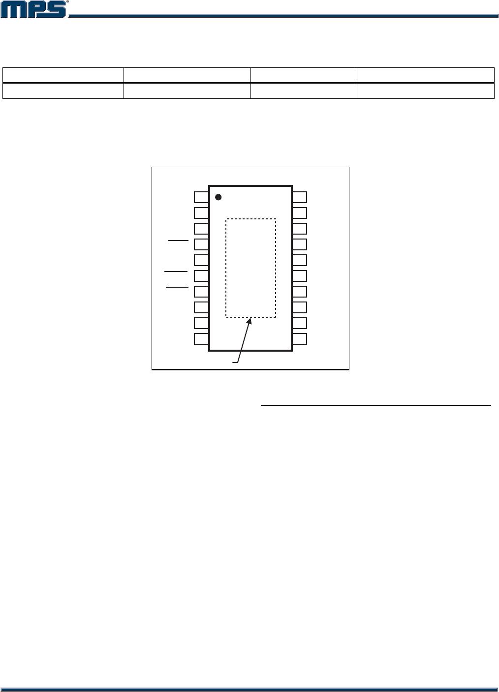
PACKAGE REFERENCE
NC
AGND1
PWM1
STBY
PWM2
FAULT
SHDN
AGND2
NC
VDR2
1
2
3
4
5
6
7
8
9
10
20
19
18
17
16
15
14
13
12
11
VDR1
BST1
PGND1
OUT1
VDD1
NC
VDD2
OUT2
PGND2
BST2
TOP VIEW
EXPOSED PAD
ABSOLUTE MAXIMUM RATINGS
(1)
VDD1/2 Supply Voltage ............................... 26V
OUT1/2 Pin Voltage............ –0.3V to V
DD
+ 0.3V
OUT1/2 to BST1/2 .........................–0.3V to +6V
Voltage at All Other Pins................–0.3V to +6V
Continuous Power Dissipation (T
A
= +25°C)
(2)
………………………………………………....3.1W
Storage Temperature.............. –55°C to +150°C
Junction Temperature.............................150°C
Lead Temperature .................................260°C
Recommended Operating Conditions
(3)
VDD1/2 Supply Voltage ...................7.5V to 24V
Peak Output Current......................5A Maximum
Operating Junct. Temp (T
J
)...... -40°C to +125°C
Thermal Resistance
(4)
θ
JA
θ
JC
TSSOP20F..............................40 ....... 6.... °C/W
Notes:
1) Exceeding these ratings may damage the device.
2) The maximum allowable power dissipation is a function of the
maximum junction temperature T
J
(MAX), the junction-to-
ambient thermal resistance
JA
, and the ambient temperature
T
A
. The maximum allowable continuous power dissipation at
any ambient temperature is calculated by P
D
(MAX) = (T
J
(MAX)-T
A
)/
JA
. Exceeding the maximum allowable powe
r
dissipation will cause excessive die temperature, and the
regulator will go into thermal shutdown. Internal thermal
shutdown circuitry protects the device from permanent
damage.
3) The device is not guaranteed to function outside of its
operating conditions.
4) Measured on approximately 1” square of 1 oz copper.
MP8042 –24V, 5A DUAL CHANNEL POWER HALF-BRIDGE
MP8042 Rev. 0.91 www.MonolithicPower.com 3
5/5/2010 MPS Proprietary Information. Unauthorized Photocopy and Duplication Prohibited.
© 2010 MPS. All Rights Reserved.
ELECTRICAL CHARACTERISTICS
V
DD1
= V
DD2
= 12V,
SHDN
V
= 5V, T
A
= +25°C, unless otherwise specified.
Parameters Symbol Condition Min Typ Max Units
VDD Operating Current I
LOAD
= 0A 2.1 2.5 mA
VDD Shutdown Current
SHDN
V
= 0V
4.0 10 µA
VDD Operating Threshold, Low 5.8 6.1 V
VDD Operating Threshold, High 6.63 7.2 V
STBY Threshold, Low
1.0 1.2 V
STBY Threshold, High
1.85 2.0 V
SHDN Threshold, Low
1.0 1.2 V
SHDN Threshold, High
1.9 2.0 V
PWM
1,2
Threshold, Low 1.5 1.69 V
PWM
1,2
Threshold, High 1.83 2.0 V
PWM Input Bias Current 1 µA
OUT On Resistance
(5)
V
DD
= 7.5V, High-Side and
Low-Side
0.15
V
PWM
= 5, Sinking 5 A
OUT Current Limit
(5)
V
PWM
= 0, Sourcing 5 A
OUT Switching Frequency
V
PWM
= 0 to 2V, 50% Duty
Cycle
0.6 MHz
OUT Maximum Duty Cycle
(6)
V
DD
= 7.5V, V
PWM
= 2V,
C
BST
= 100nF, f
SW
= 3.3kHz
99.5 %
OUT Rise/Fall Time
(5)
V
PWM
= 0V to 5V 10 ns
PWM Pulse Width
V
PWM
= 0V to 2V, High or Low
Pulse
200 ns
Dead Time
(5)
I
OUT
= ±100mA 30 ns
PWM to OUT Delay Time Rising V
PWM
= 0V to 5V 37 45 ns
PWM to OUT Delay Time Falling V
PWM
= 5 to 0V 54 65 ns
Thermal Shutdown Temperature
(5)
T
J
Rising, Hysteresis = 20°C 150
°C
Notes:
5) Not production tested.
6) OUT drives low for 1.5µs every 300µs to charge the BST to SW capacitor.

MP8042DF-LF

Mfr. #:
Manufacturer:
Monolithic Power Systems (MPS)
Description:
Gate Drivers 5A, 24V 2-Ch Power Half Bridge
Lifecycle:
New from this manufacturer.
Delivery:
DHL FedEx Ups TNT EMS
Payment:
T/T Paypal Visa MoneyGram Western Union

Products related to this Datasheet