MT9V024/D
www.onsemi.com
10
clocks out the register data 8 bits at a time. The master sends
an acknowledge bit after each 8−bit transfer. The register
address is automatically incremented after every 16 bits is
transferred. The data transfer is stopped when the master
sends a no−acknowledge bit. The MT9V024 allows for 8−bit
data transfers through the two−wire serial interface by
writing (or reading) the most significant 8 bits to the register
and then writing (or reading) the least significant 8 bits to
byte−wise address register (0x0F0).
Bus Idle State
The bus is idle when both the data and clock lines are
HIGH. Control of the bus is initiated with a start bit, and the
bus is released with a stop bit. Only the master can generate
the start and stop bits.
Table 6. SLAVE ADDRESS MODES
{S_CTRL_ADR1, S_CTRL_ADR0} Slave Address Write/Read Mode
00
0x90 Write
0x91 Read
01
0x98 Write
0x99 Read
10
0xB0 Write
0xB1 Read
11
0xB8 Write
0xB9 Read
Data Bit Transfer
One data bit is transferred during each clock pulse. The
two−wire serial interface clock pulse is provided by the
master. The data must be stable during the HIGH period of
the serial clock−it can only change when the two−wire serial
interface clock is LOW. Data is transferred 8 bits at a time,
followed by an acknowledge bit.
TWO−WIRE SERIAL INTERFACE SAMPLE READ AND WRITE SEQUENCES
16−Bit Write Sequence
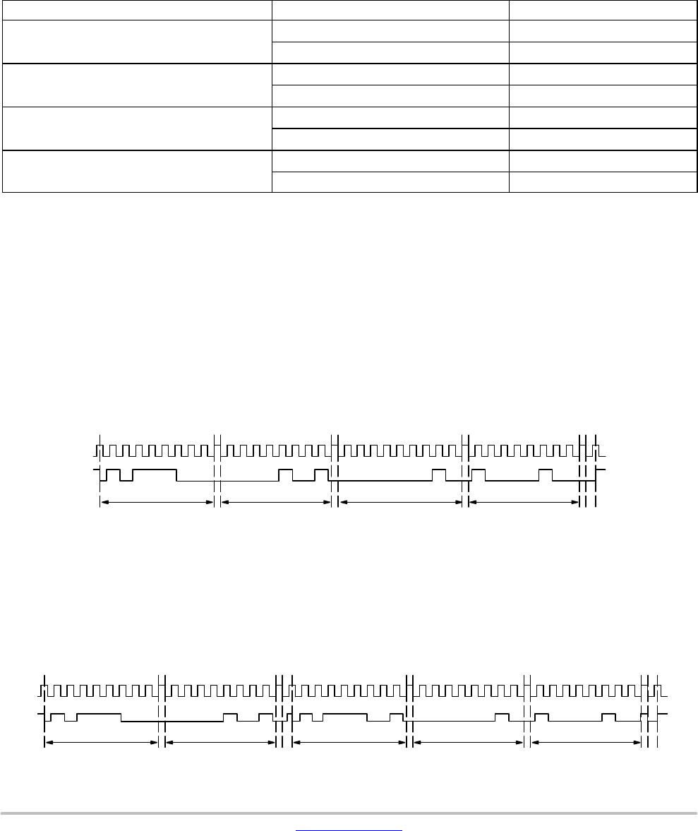
A typical write sequence for writing 16 bits to a register
is shown in Figure 10. A start bit given by the master,
followed by the write address, starts the sequence. The
image sensor then gives an acknowledge bit and expects the
register address to come first, followed by the 16−bit data.
After each 8−bit word is sent, the image sensor gives an
acknowledge bit. All 16 bits must be written before the
register is updated. After 16 bits are transferred, the register
address is automatically incremented, so that the next 16 bits
are written to the next register. The master stops writing by
sending a start or stop bit.
Figure 10. Timing Diagram Showing a Write to R0x09 with Value 0x0284
SCLK
START ACK
0xB8 ADDR 0000 0010
R0x09
ACK ACK ACK
STOP
1000 0100
S
DATA
16−Bit Read Sequence
A typical read sequence is shown in Figure 11. First the
master has to write the register address, as in a write
sequence. Then a start bit and the read address specify that
a read is about to happen from the register. The master then
clocks out the register data 8 bits at a time. The master sends
an acknowledge bit after each 8−bit transfer. The register
address is auto−incremented after every 16 bits is
transferred. The data transfer is stopped when the master
sends a no−acknowledge bit.
Figure 11. Timing Diagram Showing a Read from R0x09; Returned Value 0x0284
SCLK
START ACK
0xB8 ADDR 0xB9 ADDR 0000 0010
R0x09
ACK ACK ACK
STOP
1000 0100
NACK
S
DATA

