MT9V024/D
www.onsemi.com
38
Appendix A: Power−On Reset and Standby Timing
There are no constraints concerning the order in which the
various power supplies are applied; however, the MT9V024
requires reset to operate properly at power−up. Refer to
Figure 50 for the power−up, reset, and standby sequences.
Low−Power Non−Low−PowerNon−Low−Power
Active Pre−Standby Standby Active
Wake
up
Power
down
MIN 20 SYSCLK cycles
Note 3
MIN 20 SYSCLK cycles
MIN 20 SYSCLK cycles
Does not
respond to
serial
Interface
when
STANDBY=1
D
OUT
[9:0]
Driven = 0
Driven = 0
Power
up
V
DD
, V
DD
LVDS,
V
AA
, VAAPIX
RESET_BAR
STANDBY
SYSCLK
MIN 10 SYSCLK cycles
SCLK, S
DATA
Twi−wire Serial I/F
D
OUT
[9:0]
DATA OUTPUT
Figure 50. Power−up, Reset, Clock, and Standby Sequence
NOTES: 1. All output signals are defined during initial power−up with RESET_BAR held LOW without SYSCLK being active. To
properly reset the rest of the sensor, during initial power−up, assert RESET_BAR (set to LOW state) for at least 750ns
after all power supplies have stabilized and SYSCLK is active (being clocked). Driving RESET_BAR to LOW state does
not put the part in a low power state.
2. Before using two−wire serial interface, wait for 10 SYSCLK rising edges after RESET_BAR is de−asserted.
3. Once the sensor detects that STANDBY has been asserted, it completes the current frame readout before entering
standby mode. The user must supply enough SYSCLKs to allow a complete frame readout. See Table 2, “Frame Time,”
for more information
4. In standby, all video data and synchronization output signals are driven to a low state.
5. In standby, the two−wire serial interface is not active.
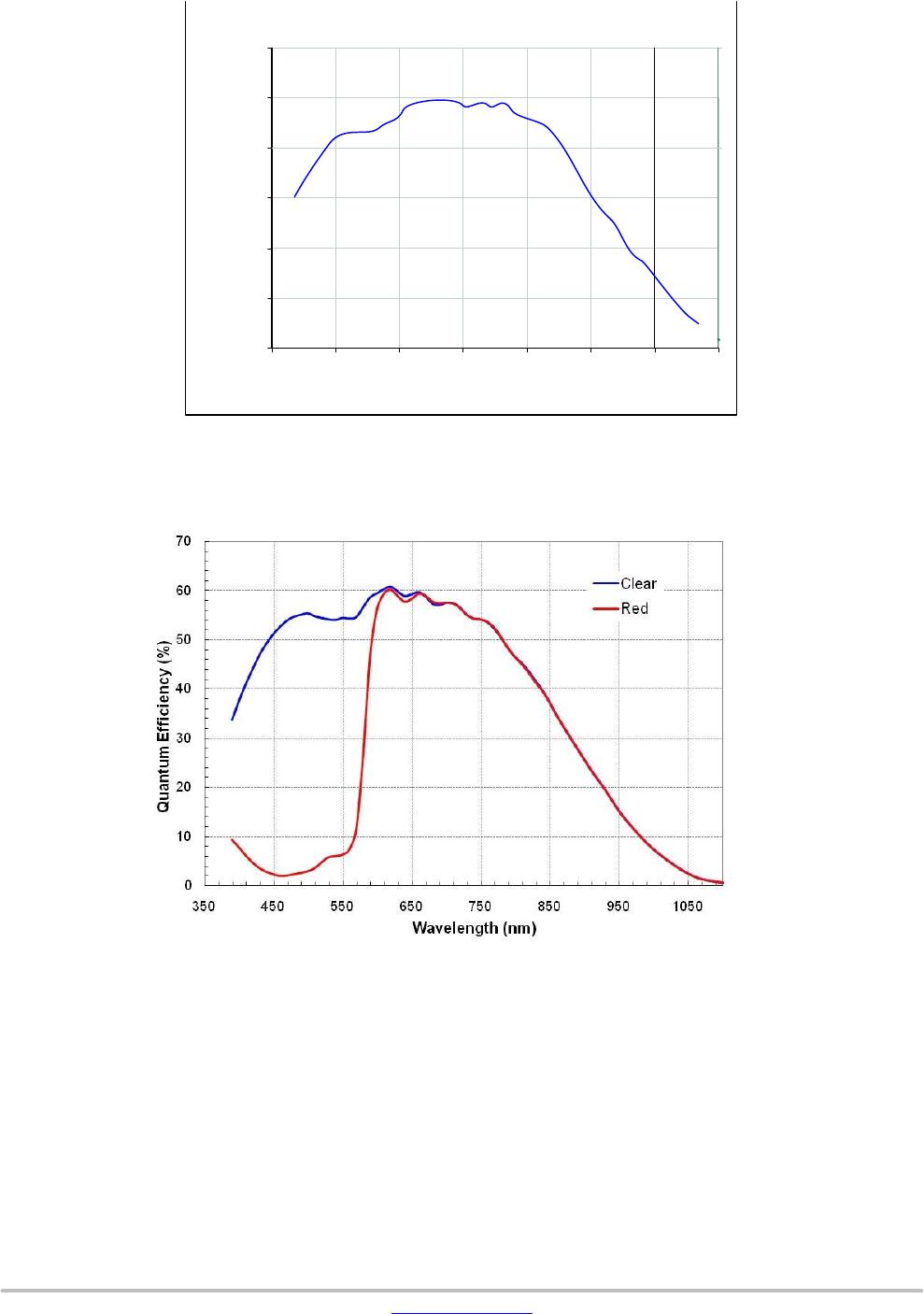
APPENDIX B: ELECTRICAL IDENTIFICATION
OF CFA TYPE
In order to identify the CFA type (RGB Bayer,
Monochrome, RCCC) that a specific MT9V024 has been,
the following table may be used.
CFA R0x6B[11:9] R0x6B[8:0]
RGB 6 4
RCCC 5 4
Mono 0 4