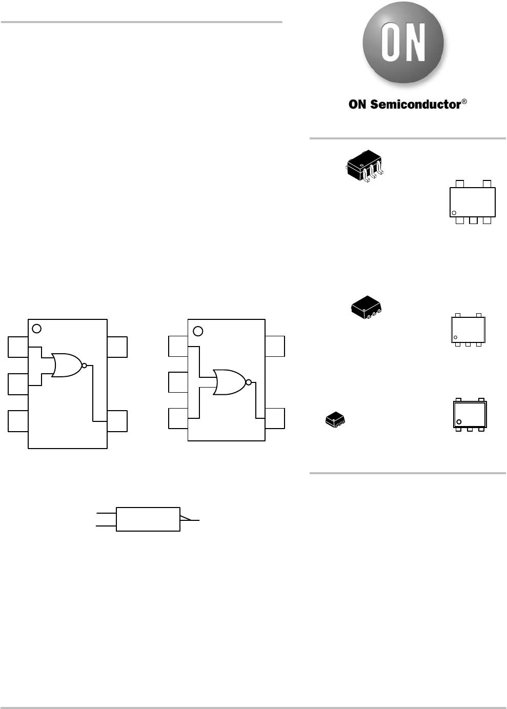
NL17SZ02
http://onsemi.com
2
PIN ASSIGNMENT
(SOT−353/SC70−5/SC−88A/SOT−553)
Pin
1
2
3
4
5
Function
A
B
GND
Y
V
CC
Input
FUNCTION TABLE
B
L
H
L
H
Output
Y = A + B
Y
H
L
L
L
A
L
L
H
H
PIN ASSIGNMENT (SOT−953)
Pin
1
2
3
4
5
Function
IN A
GND
IN B
OUT Y
V
CC
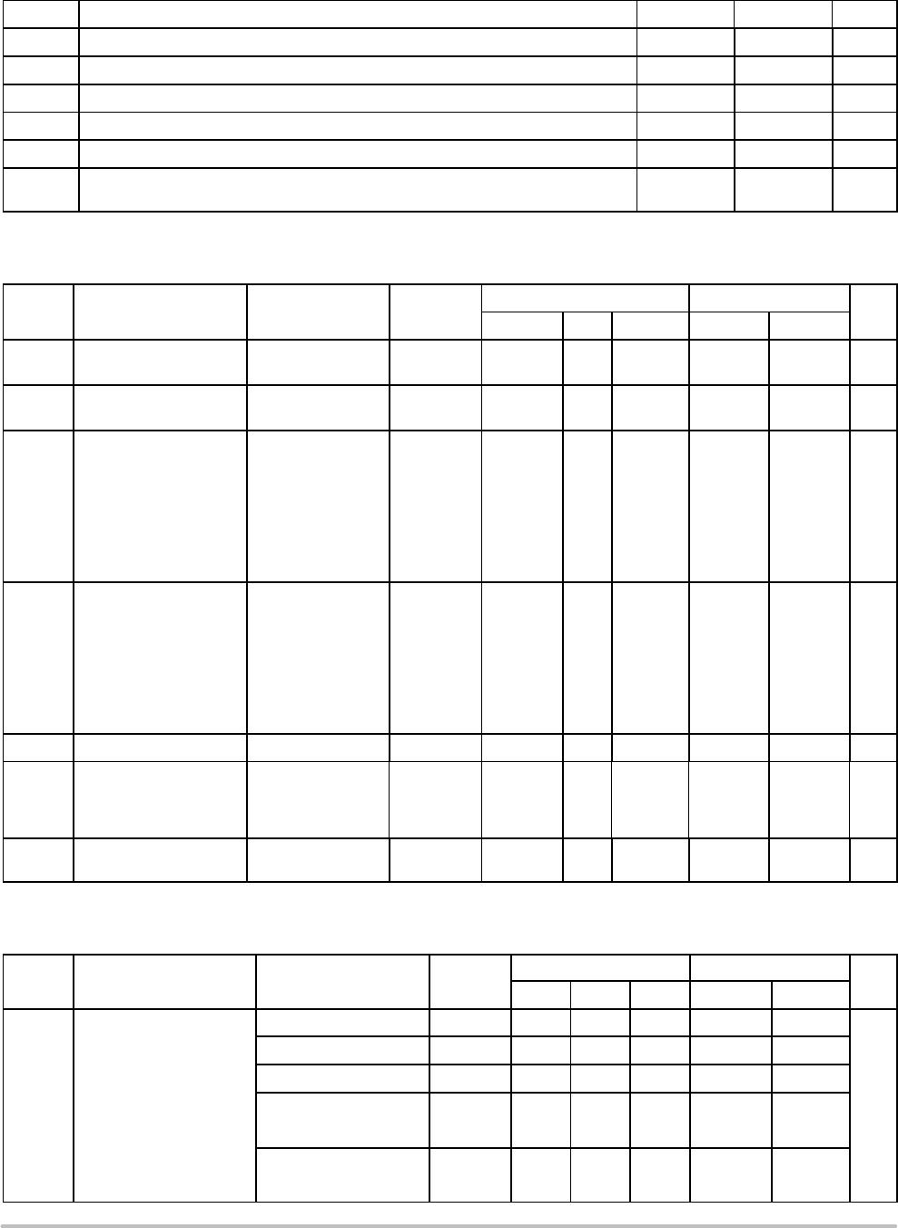
MAXIMUM RATINGS
Symbol Parameter Value Unit
V
CC
DC Supply Voltage −0.5 to )7.0 V
V
IN
DC Input Voltage −0.5 to )7.0 V
V
OUT
DC Output Voltage (SOT−353/SC70−5/SC−88A/SOT−553 Packages) −0.5 to V
CC
+ 0.5 V
V
OUT
DC Output Voltage Output at High or Low State
(SOT−953 Package) Power−Down Mode (V
CC
= 0 V)
−0.5 to V
CC
+ 0.5
−0.5 to + 0.5
V
I
IK
DC Input Diode Current −50 mA
I
OK
DC Output Diode Current V
OUT
< GND, V
OUT
> V
CC
(SOT−353/SC70−5/SC−88A/SOT−553 Packages)
±50 mA
I
OK
DC Output Diode Current (SOT−953 Package) V
OUT
< GND −50 mA
I
OUT
DC Output Sink Current ±50 mA
I
CC
DC Supply Current per Supply Pin ±100 mA
T
STG
Storage Temperature Range −65 to )150 °C
T
L
Lead Temperature, 1 mm from Case for 10 Seconds 260 °C
T
J
Junction Temperature Under Bias +150 °C
q
JA
Thermal Resistance SOT−353 (Note 1)
SOT−553
350
496
°C/W
P
D
Power Dissipation in Still Air at 85°CSOT−353
SOT−553
186
135
mW
MSL Moisture Sensitivity Level 1
F
R
Flammability Rating Oxygen Index: 28 to 34 UL 94 V−0 @ 0.125 in
ESD ESD Classification Human Body Model (Note 2)
Machine Model (Note 3)
Charged Device Model (Note 4)
Class 2
Class A
N/A
I
LATCHUP
Latchup Performance Above V
CC
and Below GND at 125°C (Note 5) ±100 mA
Stresses exceeding those listed in the Maximum Ratings table may damage the device. If any of these limits are exceeded, device functionality
should not be assumed, damage may occur and reliability may be affected.
1. Measured with minimum pad spacing on an FR4 board, using 10 mm−by−1 inch, 2−ounce copper trace with no air flow.
2. Tested to EIA/JESD22−A114−A, rated to EIA/JESD22−A114−B.
3. Tested to EIA/JESD22−A115−A, rated to EIA/JESD22−A115−A.
4. Tested to JESD22−C101−A.
5. Tested to EIA/JESD78.