NLV17SZ02DFT2G

NL17SZ02
http://onsemi.com
4
CAPACITIVE CHARACTERISTICS
Symbol Parameter Condition Typical Unit
C
IN
Input Capacitance V
CC
= 5.5 V, V
I
= 0 V or V
CC
u4 pF
C
PD
Power Dissipation Capacitance
(Note 6)
10 MHz, V
CC
= 3.3 V, V
I
= 0 V or V
CC
25
pF
10 MHz, V
CC
= 5.5 V, V
I
= 0 V or V
CC
30
6. C
PD
is defined as the value of the internal equivalent capacitance which is calculated from the operating current consumption without load.
Average operating current can be obtained by the equation: I
CC(OPR
)
= C
PD
V
CC
f
in
+ I
CC
. C
PD
is used to determine the noload dynamic
power consumption; P
D
= C
PD
V
CC
2
f
in
+ I
CC
V
CC
.
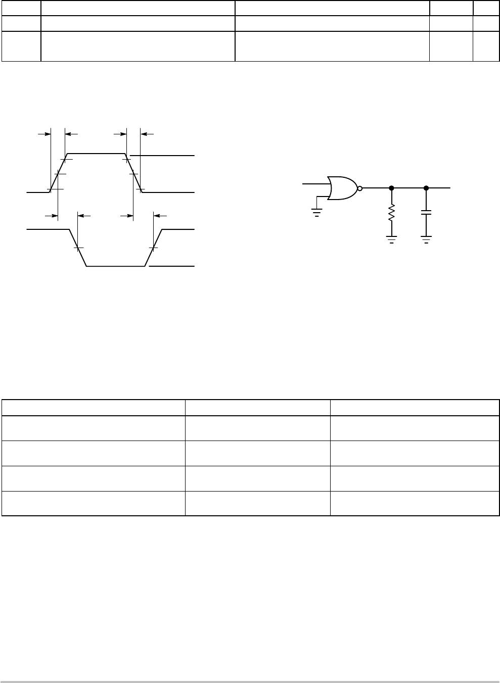
Figure 3. Switching Waveform
R
L
C
L
A 1MHz square input wave is recommended for
propagation delay tests.
Figure 4. Test Circuit
t
f
= 3 ns
V
CC
GND
V
OH
V
OL
90%
50%
10%
50%
t
PLH
t
PHL
OUTPUT Y
INPUT
A and B
t
f
= 3 ns
90%
50%
10%
50%
OUTPUT
INPUT
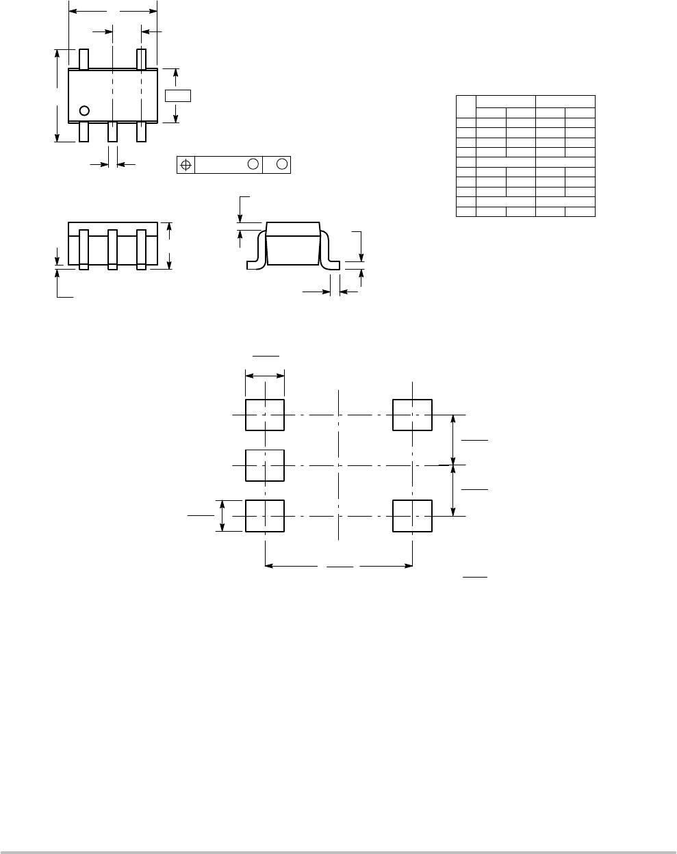
ORDERING INFORMATION
Device Package Shipping
NL17SZ02DFT2G SC88A/SOT353/SC705
(PbFree)
3000 / Tape & Reel
NLV17SZ02DFT2G* SC88A/SOT353/SC705
(PbFree)
3000 / Tape & Reel
NL17SZ02XV5T2G SOT553
(PbFree)
4000 / Tape & Reel
NL17SZ02P5T5G SOT953
(PbFree)
8000 / Tape & Reel
For information on tape and reel specifications, including part orientation and tape sizes, please refer to our Tape and Reel Packaging
Specifications Brochure, BRD8011/D.
*NLV Prefix for Automotive and Other Applications Requiring Unique Site and Control Change Requirements; AECQ100 Qualified and PPAP
Capable.
NL17SZ02
http://onsemi.com
5
PACKAGE DIMENSIONS
NOTES:
1. DIMENSIONING AND TOLERANCING
PER ANSI Y14.5M, 1982.
2. CONTROLLING DIMENSION: INCH.
3. 419A01 OBSOLETE. NEW STANDARD
419A02.
4. DIMENSIONS A AND B DO NOT INCLUDE
MOLD FLASH, PROTRUSIONS, OR GATE
BURRS.
DIM
A
MIN MAX MIN MAX
MILLIMETERS
1.80 2.200.071 0.087
INCHES
B 1.15 1.350.045 0.053
C 0.80 1.100.031 0.043
D 0.10 0.300.004 0.012
G 0.65 BSC0.026 BSC
H --- 0.10---0.004
J 0.10 0.250.004 0.010
K 0.10 0.300.004 0.012
N 0.20 REF0.008 REF
S 2.00 2.200.079 0.087
B0.2 (0.008)
MM
12 3
45
A
G
S
D
5 PL
H
C
N
J
K
B
SC88A (SC705/SOT353)
CASE 419A02
ISSUE L
ǒ
mm
inches
Ǔ
SCALE 20:1
0.65
0.025
0.65
0.025
0.50
0.0197
0.40
0.0157
1.9
0.0748
SOLDER FOOTPRINT*
*For additional information on our PbFree strategy and soldering
details, please download the ON Semiconductor Soldering and
Mounting Techniques Reference Manual, SOLDERRM/D.
NL17SZ02
http://onsemi.com
6
PACKAGE DIMENSIONS
SOT553
XV5 SUFFIX
CASE 463B
ISSUE B
1.35
0.0531
0.5
0.0197
ǒ
mm
inches
Ǔ
SCALE 20:1
0.5
0.0197
1.0
0.0394
0.45
0.0177
0.3
0.0118
*For additional information on our PbFree strategy and soldering
details, please download the ON Semiconductor Soldering and
Mounting Techniques Reference Manual, SOLDERRM/D.
SOLDERING FOOTPRINT*
e
M
0.08 (0.003) X
b
5 PL
A
c
X
Y
NOTES:
1. DIMENSIONING AND TOLERANCING PER ANSI Y14.5M, 1982.
2. CONTROLLING DIMENSION: MILLIMETERS
3. MAXIMUM LEAD THICKNESS INCLUDES LEAD FINISH
THICKNESS. MINIMUM LEAD THICKNESS IS THE MINIMUM
THICKNESS OF BASE MATERIAL.
D
E
Y
12 3
45
L
H
E
DIM
A
MIN NOM MAX MIN
MILLIMETERS
0.50 0.55 0.60 0.020
INCHES
b 0.17 0.22 0.27 0.007
c
D 1.50 1.60 1.70 0.059
E 1.10 1.20 1.30 0.043
e 0.50 BSC
L 0.10 0.20 0.30 0.004
0.022 0.024
0.009 0.011
0.063 0.067
0.047 0.051
0.008 0.012
NOM MAX
1.50 1.60 1.70 0.059 0.063 0.067
H
E
0.08 0.13 0.18
0.003 0.005 0.007
0.020 BSC

NLV17SZ02DFT2G

Mfr. #:
Manufacturer:
ON Semiconductor
Description:
Logic Gates LOG 2 INPUT NOR GATE
Lifecycle:
New from this manufacturer.
Delivery:
DHL FedEx Ups TNT EMS
Payment:
T/T Paypal Visa MoneyGram Western Union