6 DS650F1
CS4461
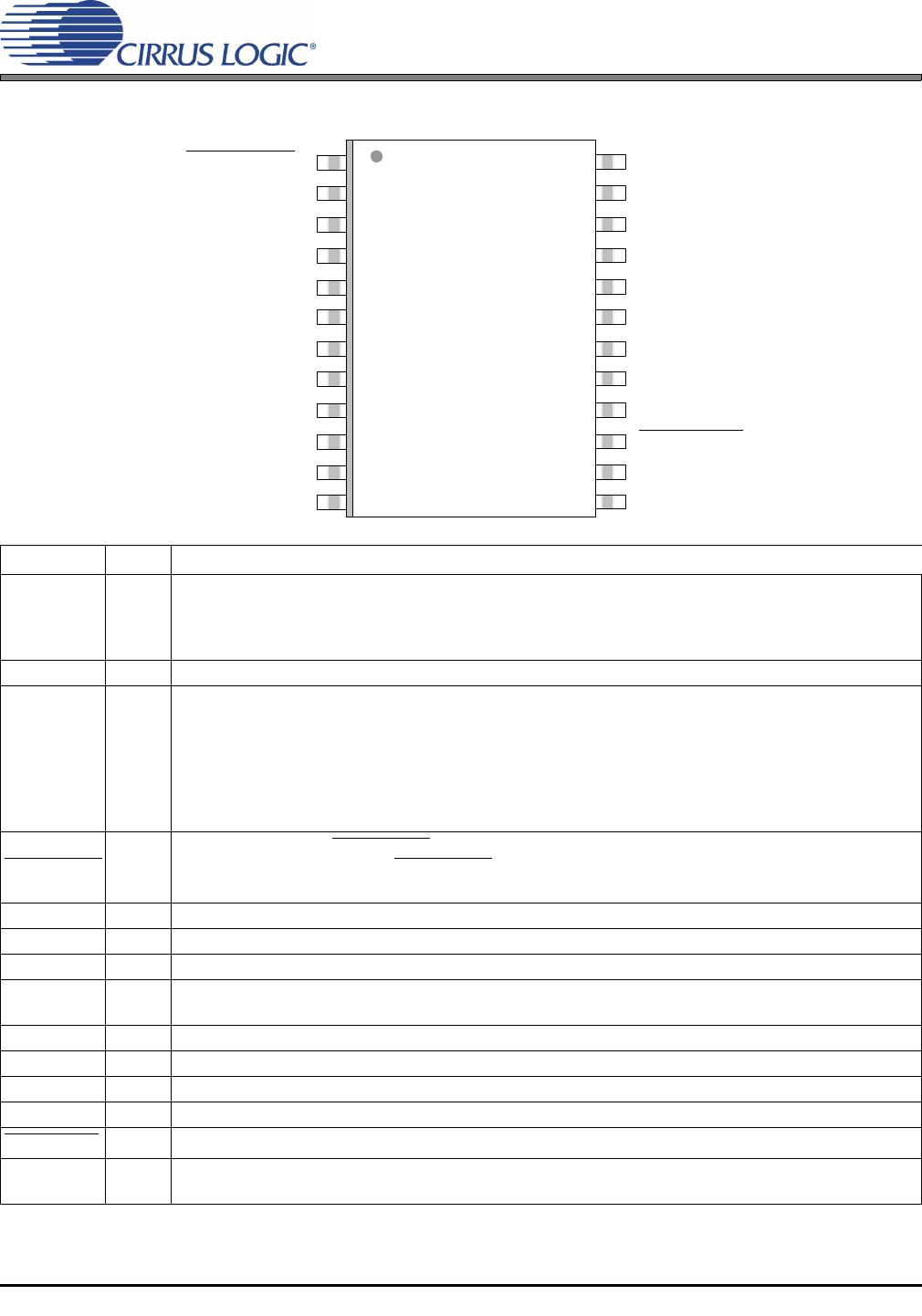
2. PIN DESCRIPTIONS
Pin Name # Pin Descriprion
VDP
6
8
13
14
Digital Logic Power (Input) – Digital core and input/output power supply. Nominally +3.3 V or +5.0 V.
Supply decoupling should placed as close as possible to pin 6.
VA 19 Analog Power (Input) - Analog power supply. Nominally +5.0 V.
GND
2
7
10
12
18
20
21
Ground (Input) - Ground reference for both analog and digital.
PSR_RESET
1
Reset (Input) - When PSR_RESET
is low, the CS4461 enters a low power mode and all internal states
are reset. On initial power up, PSR_RESET
must be held low until the power supply is stable, and all
input clocks are stable in frequency and phase.
VQ 22 Quiescent Voltage (Output) - Filter connection for the internal quiescent reference voltage.
REFGND 23 Reference Ground (Input) - Ground reference for the internal sampling circuits.
FILT+ 24 Positive Voltage Reference (Output) - Positive reference voltage for the internal sampling circuit.
AIN+
AIN-
16
17
Differential PSR Analog Input (Input) - Signals are presented differentially to the delta-sigma modula-
tor via the AIN+/- pins.
PSR_MCLK 5 Master Clock (Input) - Clock source for the delta-sigma modulator and output data.
PSR_SYNC 3 Synchronization Data Output (Output) - Used to synchronize the serial data in the PWM modulator.
PSR_DATA 4 PSR Serial Data Output (Output) - Power supply modulated and formatted serial data.
PSR_EN 11 PSR Enable (Input) - A high to low transition on this pin will enable the PSR feedback circuit.
OVERFLOW
15 Overflow (Output, open drain) - Indicates a modulator overflow condition.
TEST 9
Test (Output) - This pin may toggle during normal operation and should be pulled low through a 47 kΩ
resistor to GND in order to minimize noise.
PSR_RESET FILT+
GND REFGND
PSR_SYNC VQ
PSR_DATA GND
PSR_MCLK GND
VDP VA
GND GND
VDP AIN-
TEST AIN+
GND OVERFLOW
PSR_EN VDP
GND VDP
1
2
3
4
5
6
7
817
18
19
20
21
22
23
24
9
10
11
12 13
14
15
16
Top-Down View
24-pin TSSOP Package