BAT46WJ All information provided in this document is subject to legal disclaimers. © NXP B.V. 2011. All rights reserved.
Product data sheet Rev. 2 — 8 November 2011 6 of 12
NXP Semiconductors
BAT46WJ
Single Schottky barrier diode
T
j
= 125 C
(1) =1
(2) =0.9
(3) =0.8
(4) =0.5
FR4 PCB, standard footprint
T
j
= 150 C
(1) =1; DC
(2) = 0.5; f = 20 kHz
(3) = 0.2; f = 20 kHz
(4) = 0.1; f = 20 kHz
Fig 6. Average reverse power dissipation as a
function of reverse voltage; typical values
Fig 7. Average forward current as a function of
ambient temperature; typical values
FR4 PCB, mounting pad for cathode 1 cm
2
T
j
= 150 C
(1) =1; DC
(2) = 0.5; f = 20 kHz
(3) = 0.2; f = 20 kHz
(4) = 0.1; f = 20 kHz
T
j
= 150 C
(1) =1; DC
(2) = 0.5; f = 20 kHz
(3) = 0.2; f = 20 kHz
(4) = 0.1; f = 20 kHz
Fig 8. Average forward current as a function of
ambient temperature; typical values
Fig 9. Average forward current as a function of
solder point temperature; typical values
BAT46WJ All information provided in this document is subject to legal disclaimers. © NXP B.V. 2011. All rights reserved.
Product data sheet Rev. 2 — 8 November 2011 7 of 12
NXP Semiconductors
BAT46WJ
Single Schottky barrier diode
8. Test information
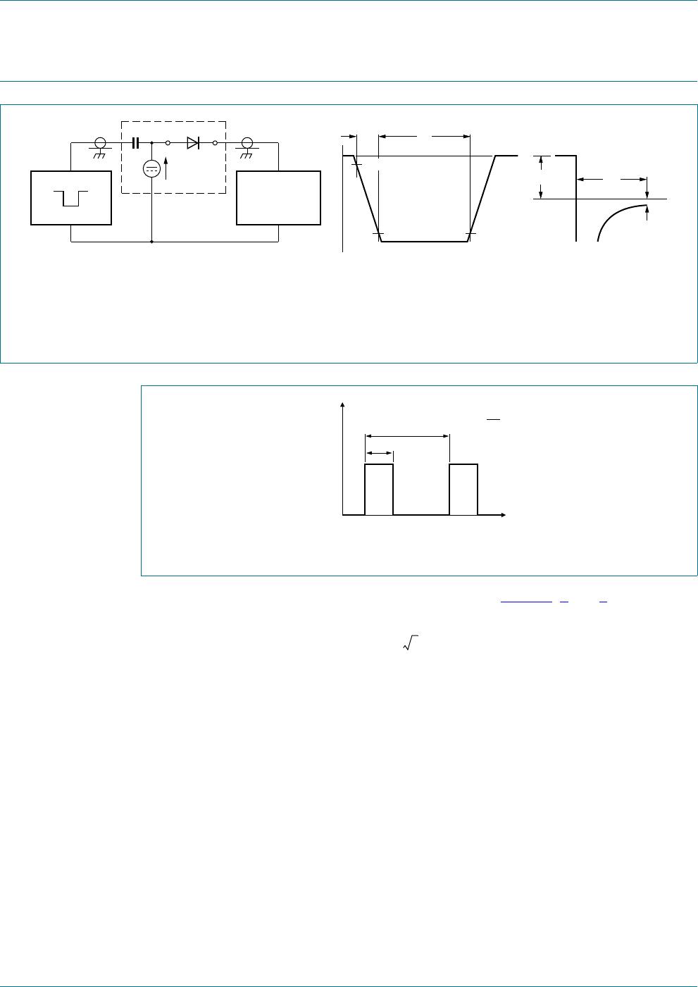
The current ratings for the typical waveforms as shown in Figure 7, 8 and 9 are
calculated according to the equations: with I
M
defined as peak current,
at DC, and with I
RMS
defined as RMS current.
8.1 Quality information
This product has been qualified in accordance with the Automotive Electronics Council
(AEC) standard Q101 - Stress test qualification for discrete semiconductors, and is
suitable for use in automotive applications.
(1) I
R
=1mA
Input signal: reverse pulse rise time t
r
= 0.6 ns; reverse voltage pulse duration t
p
= 100 ns; duty cycle =0.05
Oscilloscope: rise time t
r
=0.35ns
Fig 10. Reverse recovery time test circuit and waveforms
t
rr
(1)
+ I
F
t
output signal
t
r
t
p
t
10 %
90 %
V
R
input signal
V = V
R
+
I
F
×
R
S
R
S
= 50
Ω
I
F
D.U.T.
R
i
= 50
Ω
SAMPLING
OSCILLOSCOPE
mga881
Fig 11. Duty cycle definition
t
1
t
2
P
t
006aaa812
duty cycle δ =
t
1
t
2
I
FAV
I
M
=
I
RMS
I
FAV
=
I
RMS
I
M
=
BAT46WJ All information provided in this document is subject to legal disclaimers. © NXP B.V. 2011. All rights reserved.
Product data sheet Rev. 2 — 8 November 2011 8 of 12
NXP Semiconductors
BAT46WJ
Single Schottky barrier diode
9. Package outline
10. Packing information
[1] For further information and the availability of packing methods, see Section 14.
11. Soldering
Fig 12. Package outline SOD323F (SC-90)
04-09-13Dimensions in mm
0.80
0.65
0.25
0.10
0.5
0.3
2.7
2.3
1.8
1.6
0.40
0.25
1.35
1.15
1
2
Table 8. Packing methods
The indicated -xxx are the last three digits of the 12NC ordering code.
[1]
Type number Package Description Packing quantity
3000 10000
BAT46WJ SOD323F 4 mm pitch, 8 mm tape and reel -115 -135
Reflow soldering is the only recommended soldering method.
Fig 13. Reflow soldering footprint SOD323F (SC-90)
0.951.65
2.2
2.1
3.05
solder lands
solder resist
occupied area
solder paste
Dimensions in mm
0.5
(2×)
0.6
(2×)
0.6 (2×)0.5 (2×)
sod323f_fr

BAT46WJ,115

Mfr. #:
Manufacturer:
Nexperia
Description:
Schottky Diodes & Rectifiers Schottky Diodes 100V 250mA Single
Lifecycle:
New from this manufacturer.
Delivery:
DHL FedEx Ups TNT EMS
Payment:
T/T Paypal Visa MoneyGram Western Union

Products related to this Datasheet