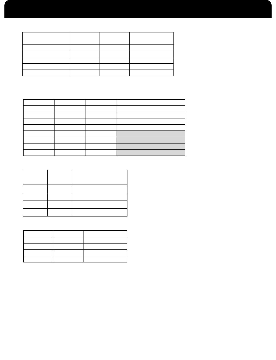
PARAMETER SYMBOL CONDITIONS MIN TYP MAX UNITS NOTES
MHz 2,3
MHz 2,3
ppm
SSof f
PCIe 100MHz or 125MHz ppm 1,2
ppm
SSon
PCIe @ -0.5% spread, 100MHz only ppm 1,2
Rising/Falling Edge Slew Rate t
SLEW
Differential Measurement 2.2 4.1 5.7 V/ns 1,3,6
Slew Rate Variation t
SLVAR
Single-ended Measurement 1 20 % 1,6
Maximum Output Voltage V
HIGH
Includes overshoot 793 1150 mV 6,7
Minimum Output Voltage V
LOW
Includes undershoot -300 -22 mV 6,7
Differential Voltage Swing V
SWING
Differential Measurement 300 mV 1,6
Crossing Point Voltage V
XABS
Single-ended Measurement 300 419 550 mV 1,4,6
Crossing Point Variation V
XABSVAR
Single-ended Measurement 115 140 mV 1,4,5
Duty Cycle D
CYC
Differential Measurement 45 50.1 55 % 1
PCIe Jitter - Cycle to Cycle PCIe
JC2C
Differential Measurement 36 125 ps 1
PCIe[5:0] Skew T
SKEwPCIe50
Differential Measurement 1172 1500 ps 1,6,8
Spread Spectrum Modulation
Frequency
f
SSMOD
Triangular Modulation 30 31.5 33 kHz
Notes for PCIe Clocks:
1
Guaranteed by design and characterization, not 100% tested in production.
2
Clock Frequency specifications are guaranteed assuming that REF is at 25MHz
3
Slew rate measured through V_swing voltage range centered about differential zero
4
Vcross is defined at the voltage where Clock = Clock#.
5
Only applies to the differential rising edge (Clock rising, Clock# falling.)
6
At default SMBus settings.
7
The Freescale P-series CPU's have internal terminations on their SerDes Reference Clock inputs. The resulting amplitude at these inputs will be 1/2 of the
values listed, which are well within the 800mV Freescale specification for these inputs.
8
This value includes an intentional output-to-output skew of approximately 250ps.
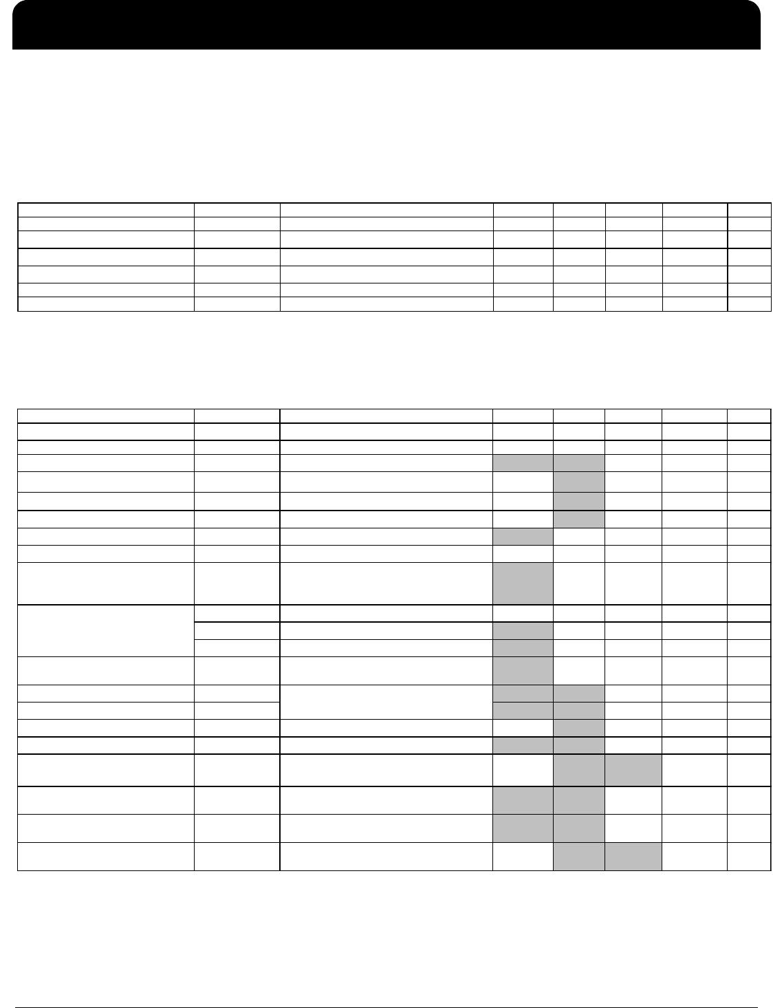
Synthesis error
0
+/-100
Clock Frequency f Spread off
100.00
125.00
.com for complete specs. Guaranteed by desi