IDT6V49205A
FREESCALE P10XX AND P20XX SYSTEM CLOCK W/66.66M DDR CLOCK
IDT®
FREESCALE P10XX AND P20XX SYSTEM CLOCK W/66.66M DDR CLOCK 7
IDT6V49205A
REV Q 112316
Electrical Characteristics - DDR Clock
Electrical Characteristics - Sys_CCB
Electrical Characteristics - 125M
PARAMETER SYMBOL CONDITIONS MIN TYP MAX UNITS NOTES
DDR Clock Frequency f
DDR
V
T
= OVDD/2 V MHz 2,3,6
ppm
SSof f
Spread off ppm 1,2,5
ppm
SSon
Spread on ppm 1,2,5
Output High Voltage V
OH
V
OH
at the selected operating frequency 2.4 V 1
Output Low Voltage V
OL
V
OL
at the selected operating frequency 0.4 V 1
t
SLEW00
'00' = Hi-Z V/ns
t
SLEW01
'01' Slow Slew Rate (Averaging on) 1.1 1.6 2.3 V/ns 1,3,8
t
SLEW10
'10' Fast Slew Rate (Averaging on) 1.6 2.3 3.2 V/ns 1,3,8
t
SLEW11
'11' Fastest Slew Rate (Averaging on) 1.8 2.7 3.7 V/ns 1,3,8
Duty Cycle d
t1
V
T
= OVDD/2 V 40 51.4 60 % 1,6
Jitter, Peak period jitter t
jpeak
V
T
= OVDD/2 V ±96 ±150 ps 1,6
Phase Noise t
phasenoise
-56dBc 10 500 kHz 1,7
AC Input Swing Limits @ 3.3V
OV
DD
Δ
V
AC
This is the difference between VOL and
VOH at the selected operating frequency.
1.9 3.4 V 1
Spread Spectrum Modulation
Frequency
f
SSMOD
Triangular Modulation 30 32.3 60 kHz
66.666
Synthesis error
0
+/-150
Slew Rate
VDDO = 3.3V
Hi-Z
PARAMETER SYMBOL CONDITIONS MIN TYP MAX UNITS NOTES
Clock frequency f
125M
V
T
= OVDD/2 V ns 2,3,6
Synthesis error ppm ppm 1,2,5
Output High Voltage V
OH
V
OH
at the selected operating frequency 2.2 V 1
Output Low Voltage V
OL
V
OL
at the selected operating frequency 0.5 V 1
Rise/Fall time
VDDO = 3.3V
t
RF125M3.3V
Measured between 0.6V and 2.7V 0.7 1 ns 1,3
Duty Cycle d
t1
V
T
= OVDD/2 V 47 52 53 % 1
Jitter, Peak period jitter t
jpeak
V
T
= OVDD/2 V
±
150 ps 1
0
125.00
IDT6V49205A
FREESCALE P10XX AND P20XX SYSTEM CLOCK W/66.66M DDR CLOCK
IDT®
FREESCALE P10XX AND P20XX SYSTEM CLOCK W/66.66M DDR CLOCK 8
IDT6V49205A
REV Q 112316
Electrical Characteristics - REF(5:0)
Electrical Characteristics - USB_CLK(2:1)
Electrical Characteristics - 2.048M(1:0)
PARAMETER SYMBOL CONDITIONS MIN TYP MAX UNITS NOTES
Clock Frequency f V
T
= OVDD/2 V MHz 2,3
Crystal Frequency Error ppm Including all aging and tuning effects -50 50 ppm 1,2
Output High Voltage
V
OH
V
OH
at the selected operating frequency
2.2 V 1
Output Low Voltage V
OL
V
OL
at the selected operating frequency 0.4 V 1
Slew Rate
VDDO 3 3V
t
SLEW
'00' = Hi-Z 1.0 1.7 2.7 V/ns 1,3,4
Duty Cycle d
t1
V
T
= OVDD/2 V 40 51 60 % 1
Pin to Pin Skew t
skew
V
T
= 1.5 V, odd/even outputs have an
intentional 180degree phase shift.
ps 1
Jitter, Peak period jitter t
jpeak
V
T
= OVDD/2 V ±78 ±200 ps 1
Jitter, Phase t
jphase
(12kHz-5MHz), V
T
= 1.5 V 1.7 3 ps rms 1
N/A
25.00
IDT6V49205A
FREESCALE P10XX AND P20XX SYSTEM CLOCK W/66.66M DDR CLOCK
IDT®
FREESCALE P10XX AND P20XX SYSTEM CLOCK W/66.66M DDR CLOCK 9
IDT6V49205A
REV Q 112316
General SMBus Serial Interface Information for IDT6V49205A
How to Write
Controller (host) sends a start bit
Controller (host) sends the write address
IDT clock will acknowledge
Controller (host) sends the beginning byte location = N
IDT clock will acknowledge
Controller (host) sends the byte count = X
IDT clock will acknowledge
Controller (host) starts sending Byte N through Byte
N+X-1
IDT clock will acknowledge each byte one at a time
Controller (host) sends a Stop bit
Note: I2C compatible. Native mode is SMBus Block mode
protocol. To use I2C Byte mode set the 2^7 bit in the
command Byte. No Byte count is used.
How to Read
Controller (host) will send a start bit
Controller (host) sends the write address
IDT clock will acknowledge
Controller (host) sends the beginning byte location = N
IDT clock will acknowledge
Controller (host) will send a separate start bit
Controller (host) sends the read address
IDT clock will acknowledge
IDT clock will send the data byte count = X
IDT clock sends Byte N+X-1
IDT clock sends Byte 0 through Byte X (if X
(H)
was
written to Byte 8)
Controller (host) will need to acknowledge each byte
Controller (host) will send a not acknowledge bit
Controller (host) will send a stop bit
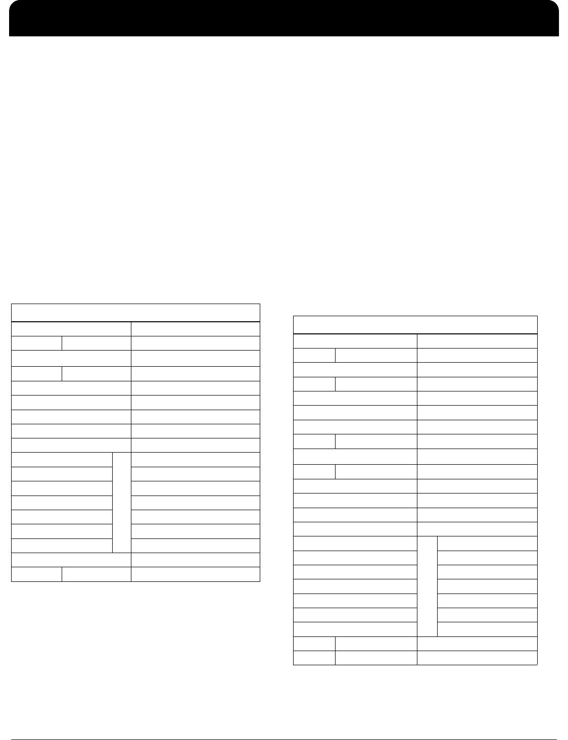
Index Block Write Operation
Controller (Host) IDT (Slave/Receiver)
TstarT bit
Slave Address D2
(H)
WR WRite
ACK
Beginning Byte = N
ACK
Data Byte Count = X
ACK
Beginning Byte N
X Byte
ACK
O
O O
O O
O
Byte N + X - 1
ACK
PstoP bit
Index Block Read Operation
Controller (Host) IDT (Slave/Receiver)
TstarT bit
Slave Address D2
(H)
WR WRite
ACK
Beginning Byte = N
ACK
RT Repeat starT
Slave Address D3
(H)
RD ReaD
ACK
Data Byte Count=X
ACK
X Byte
Beginning Byte N
ACK
O
O O
O O
O
Byte N + X - 1
N Not acknowledge
PstoP bit

6V49205APAGI

Mfr. #:
Manufacturer:
IDT
Description:
Clock Generators & Support Products QorIQ Clock Synthesi
Lifecycle:
New from this manufacturer.
Delivery:
DHL FedEx Ups TNT EMS
Payment:
T/T Paypal Visa MoneyGram Western Union

Products related to this Datasheet