Exar Corporation 48720 Kato Road, Fremont CA, 94538 (510) 668-7000 FAX (510) 668-7017 www.exar.com
XRA1405
16-BIT SPI GPIO EXPANDER WITH INTEGRATED LEVEL SHIFTERS
SEPTEMBER 2011 REV. 1.0.0
GENERAL DESCRIPTION
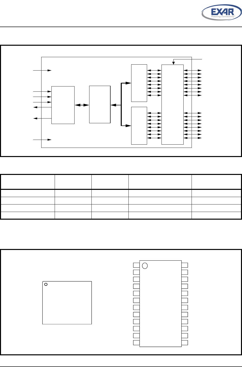
The XRA1405 is an 16-bit GPIO expander with an
SPI interface. After power-up, the XRA1405 has
internal 100K ohm pull-up resistors on each I/O pin
that can be individually enabled.
In addition, the GPIOs on the XRA1405 can
individually be controlled and configured. As outputs,
the GPIOs can be outputs that are high, low or in
three-state mode. The three-state mode feature is
useful for applications where the power is removed
from the remote devices, but they may still be
connected to the GPIO expander.
As inputs, the internal pull-up resistors can be
enabled or disabled and the input polarity can be
inverted. The interrupt can be programmed for
different behaviors. The interrupts can be
programmed to generate an interrupt on the rising
edge, falling edge or on both edges. The interrupt
can be cleared if the input changes back to its original
state or by reading the current state of the inputs.
The XRA1405 is available in 24-pin QFN and 24-pin
TSSOP packages.
FEATURES
1.65V to 3.6V operating voltage
16 General Purpose I/Os (GPIOs)
Integrated Level Shifters
5V tolerant inputs
Maximum stand-by current of 1uA at +1.8V
SPI bus interface
SPI Clock Frequency up to 26MHz
Individually programmable inputs
Internal pull-up resistors
Polarity inversion
Individual interrupt enable
Rising edge and/or Falling edge interrupt
Input filter
Individually programmable outputs
Output Level Control
Output Three-State Control
Open-drain active low interrupt output
3kV HBM ESD protection per JESD22-A114F
200mA latch-up performance per JESD78B
APPLICATIONS
Personal Digital Assistants (PDA)
Cellular Phones/Data Devices
Battery-Operated Devices
Global Positioning System (GPS)
Bluetooth
XRA1405
2
16-BIT SPI GPIO EXPANDER WITH INTEGRATED LEVEL SHIFTERS REV. 1.0.0
FIGURE 1. XRA1405 BLOCK DIAGRAM
SPI Bus
Interfa ce
VCC (1.65V – 3.6V)
GND
IR Q #
SI
SO
CS#
SCL
GPIO
Control
Registers
P0
GPIOs
P1
P2
P3
P4
P5
P6
P7
P8
GPIOs
P9
P10
P11
P12
P13
P14
P15
Integrated
Level
Shifters
(1.65V – 3.6V)
VCCP
ORDERING INFORMATION
PART NUMBER PACKAGE
NUMBER OF
GPIO
S
OPERATING TEMPERATURE
R
ANGE
DEVICE STATUS
XRA1405IL24-F QFN-24 16 -40°C to +85°C Active
XRA1405IL24TR-F QFN-24 16 -40°C to +85°C Active
XRA1405IG24-F TSSOP-24 16 -40°C to +85°C Active
XRA1405IG24TR-F TSSOP-24 16 -40°C to +85°C Active
NOTE: TR = Tape and Reel, F = Green / RoHS
FIGURE 2. PIN OUT ASSIGNMENTS
P11
XRA1405
24-Pin
TSSOP
3
5
4
7
6
8
9
10
11
12
1
2
13
14
15
16
17
18
19
20
21
22
23
24IRQ#
VCC
SI
P0
P1
P2
P3
P4
P5
P6
P7
GND
VCCP
SO
SCL
CS#
P15
P14
P13
P12
P11
P10
P9
P8
XRA1405
24-Pin QFN
78 9101112
GND
P8
P9
P10
P7
P6
17
18
13
16
14
15
P13
P14
P15
CS#
P12
24 23 22 21 20 19
2
1
6
3
5
4
P3
P2
P1
P0
P4
P5
IRQ#
VCCP
SO
SCL
VCC
SI
XRA1405
3
REV. 1.0.0 16-BIT SPI GPIO EXPANDER WITH INTEGRATED LEVEL SHIFTERS
PIN DESCRIPTIONS
Pin Description
NAME
PIN# PIN#
TYPE DESCRIPTION
SPI INTERFACE
SO 20 23 O
SPI serial data output.
SCL 19 22 I
SPI bus serial input clock.
IRQ# 22 1 OD
Interrupt output (open-drain, active LOW).
CS# 18 16 I
SPI bus chip select.
SI 24 3 I
SPI serial data input.
GPIOs
P0
P1
P2
P3
P4
P5
P6
P7
1
2
3
4
5
6
7
8
4
5
6
7
8
9
10
11
I/O
I/O
I/O
I/O
I/O
I/O
I/O
I/O
General purpose I/Os P0-P7. All GPIOs are configured as inputs upon power-
up or after a reset.
P8
P9
P10
P11
P12
P13
P14
P15
10
11
12
13
14
15
16
17
13
14
15
16
17
18
19
20
I/O
I/O
I/O
I/O
I/O
I/O
I/O
I/O
General purpose I/O P8-P15. All GPIOs are configured as inputs upon power-
up or after a reset.
ANCILLARY SIGNALS
VCCP 21 24
1.65V to 3.6V VCC supply voltage for GPIOs.
VCC 23 2 Pwr
1.65V to 3.6V VCC supply voltage for SPI bus interface.
GND 9 12 Pwr
Power supply common, ground.
GND Center
Pad
- Pwr
The exposed pad at the bottom surface of the package is designed for thermal
performance. Use of a center pad on the PCB is strongly recommended for ther
-
mal conductivity as well as to provide mechanical stability of the package on the
PCB. The center pad is recommended to be solder masked defined with open
-
ing size less than or equal to the exposed thermal pad on the package bottom to
prevent solder bridging to the outer leads of the device. Thermal vias must be
connected to GND plane as the thermal pad of package is at GND potential.
Pin type: I=Input, O=Output, I/O= Input/output, OD=Output Open Drain.
QFN-24 TSSOP-24

XRA1405IG24-F

Mfr. #:
Manufacturer:
MaxLinear
Description:
Interface - I/O Expanders 16 Bit SPI GPIO Expander
Lifecycle:
New from this manufacturer.
Delivery:
DHL FedEx Ups TNT EMS
Payment:
T/T Paypal Visa MoneyGram Western Union