XRA1405
4
16-BIT SPI GPIO EXPANDER WITH INTEGRATED LEVEL SHIFTERS REV. 1.0.0
1.0 FUNCTIONAL DESCRIPTIONS
1.1 SPI bus Interface
The SPI interface consists of four lines: serial clock (SCL), chip select (CS#), slave output (SO) and slave input
(SI). The serial clock, slave output and slave input can be as fast as 26 MHz. To access the device in the SPI
mode, the CS# signal is asserted by the SPI master, then the SPI master starts toggling the SCL signal with
the appropriate transaction information. The first bit sent by the SPI master includes whether it is a read or
write transaction and the register being accessed. See
Table 1 below.
TABLE 1: SPI COMMAND BYTE FORMAT
BIT FUNCTION
7 Read/Write#
Logic 1 = Read
Logic 0 = Write
6:1 Command Byte
0 Reserved
FIGURE 3. SPI WRITE
0 0 0 A3 A2 A1 A0 X D7 D6 D5 D4 D3 D2 D1 D0
SCL
SI
FIGURE 4. SPI READ
1
0
0A3A2
A1
A0 X
D7
D6 D5 D4 D3 D2 D1
D0
SCL
SI
SO
After the last read or write transaction, the SPI master will set the SCL signal back to its idle state (LOW).
XRA1405
5
REV. 1.0.0 16-BIT SPI GPIO EXPANDER WITH INTEGRATED LEVEL SHIFTERS
1.1.1 SPI Command Byte
An SPI command byte is sent by the SPI master following the slave address. The command byte indicates the
address offset of the register that will be accessed.
Table 2 below lists the command bytes for each register.
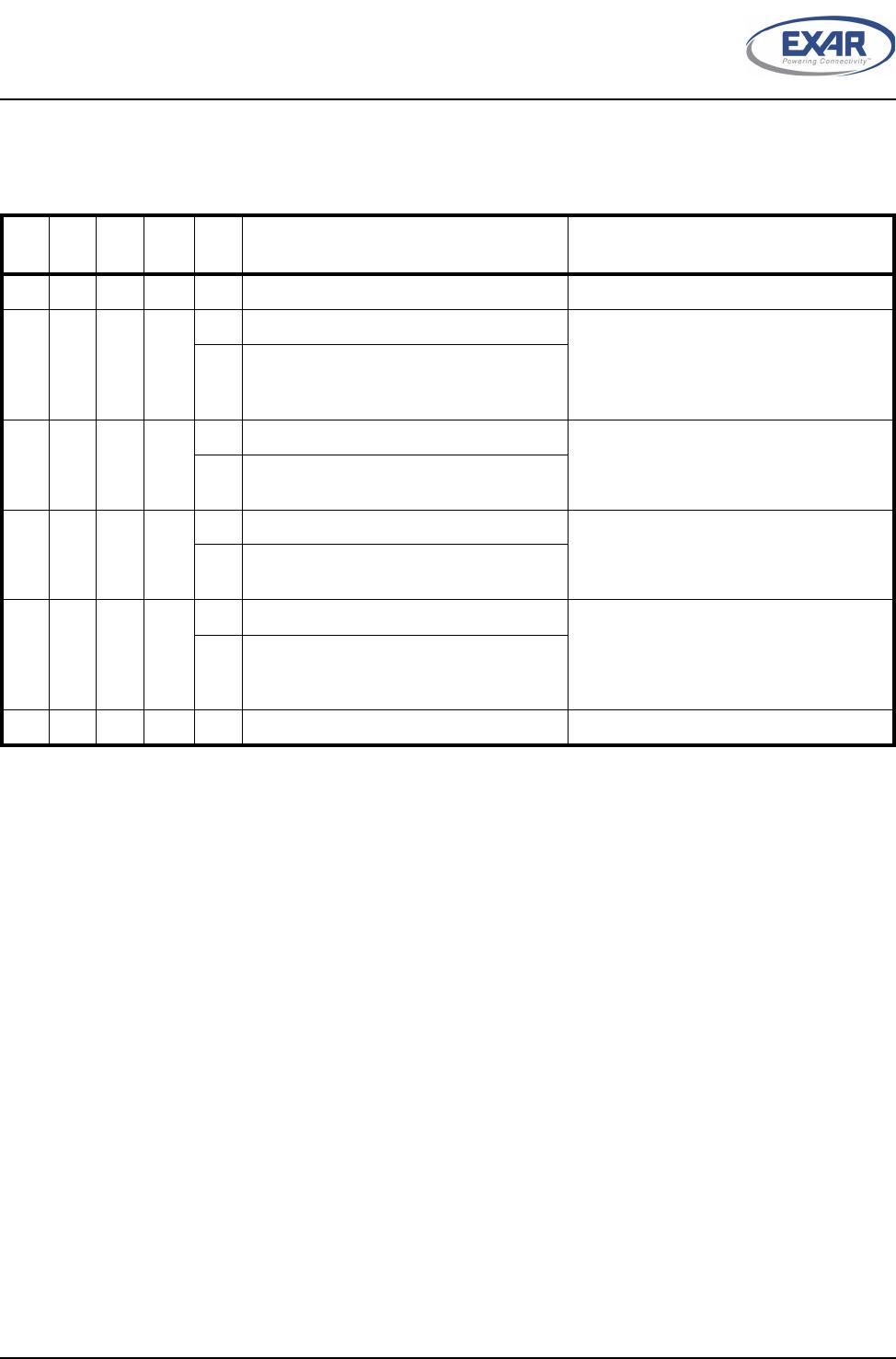
TABLE 2: COMMAND BYTE (REGISTER ADDRESS)
COMMAND BYTE REGISTER NAME DESCRIPTION READ/WRITE DEFAULT VALUES
0x00 GSR1 - GPIO State for P0-P7 Read-Only 0xXX
0x01 GSR2 - GPIO State for P8-P15 Read-Only 0xXX
0x02 OCR1 - Output Control for P0-P7 Read/Write 0xFF
0x03 OCR2 - Output Control for P8-P15 Read/Write 0xFF
0x04 PIR1 - Input Polarity Inversion for P0-P7 Read/Write 0x00
0x05 PIR2 - Input Polarity Inversion for P8-P15 Read/Write 0x00
0x06 GCR1 - GPIO Configuration for P0-P7 Read/Write 0xFF
0x07 GCR2 - GPIO Configuration for P8-P15 Read/Write 0xFF
0x08 PUR1 - Input Internal Pull-up Resistor Enable/Disable for P0-P7 Read/Write 0x00
0x09 PUR2 - Input Internal Pull-up Resistor Enable/Disable for P8-P15 Read/Write 0x00
0x0A IER1 - Input Interrupt Enable for P0-P7 Read/Write 0x00
0x0B IER2 - Input Interrupt Enable for P8-P15 Read/Write 0x00
0x0C TSCR1 - Output Three-State Control for P0-P7 Read/Write 0x00
0x0D TSCR2 - Output Three-State Control for P8-P15 Read/Write 0x00
0x0E ISR1 - Input Interrupt Status for P0-P7 Read 0x00
0x0F ISR2 - Input Interrupt Status for P8-P15 Read 0x00
0x10 REIR1 - Input Rising Edge Interrupt Enable for P0-P7 Read/Write 0x00
0x11 REIR2 - Input Rising Edge Interrupt Enable for P8-P15 Read/Write 0x00
0x12 FEIR1 - Input Falling Edge Interrupt Enable for P0-P7 Read/Write 0x00
0x13 FEIR2 - Input Falling Edge Interrupt Enable for P8-P15 Read/Write 0x00
0x14 IFR1 - Input Filter Enable/Disable for P0-P7 Read/Write 0xFF
0x15 IFR2 - Input Filter Enable/Disable for P8-P15 Read/Write 0xFF
XRA1405
6
16-BIT SPI GPIO EXPANDER WITH INTEGRATED LEVEL SHIFTERS REV. 1.0.0
1.2 Interrupts
The table below summarizes the interrupt behavior of the different register settings for the XRA1405.
TABLE 3: INTERRUPT GENERATION AND CLEARING
BIT BIT BIT BIT BIT
INTERRUPT GENERATED BY: INTERRUPT CLEARED BY:
1 0 X X X No interrupts enabled (default) N/A
1 1 0 0
0 A rising or falling edge on the input Reading the GSR register or if the input
changes back to its previous state (state of
input during last read to GSR)
1 A rising or falling edge on the input and
remains in the new state for more than
1075ns
1 1 1 0
0 A rising edge on the input Reading the GSR register
1 A rising edge on the input and remains high
for more than 1075ns
1 1 0 1
0 A falling edge on the input Reading the GSR register
1 A falling edge on the input and remains low
for more than 1075ns
1 1 1 1
0 A rising or falling edge on the input Reading the GSR register
1 A rising or falling edge on the input and
remains in the new state for more than
1075ns
0 x x x x No interrupts in output mode N/A
GCR IER REIR FEIR IFR

XRA1405IG24-F

Mfr. #:
Manufacturer:
MaxLinear
Description:
Interface - I/O Expanders 16 Bit SPI GPIO Expander
Lifecycle:
New from this manufacturer.
Delivery:
DHL FedEx Ups TNT EMS
Payment:
T/T Paypal Visa MoneyGram Western Union