Expand menu
Hello, Sign in
My Account
0
Cart
Home
Products
Sensors
Semiconductors
Passive Components
Connectors
Power
Electromechanical
Optoelectronics
Circuit Protection
Integrated Circuits - ICs
Main Products
Manufacturers
Blog
Services
About OMO
About Us
Contact Us
Check Stock
DD180N16SHPSA1
P1-P3
P4-P6
P7-P9
P10-P10
Netz-Dioden-M
odul
Rectifier Diode M
odule
Technische Informati
on
/
technical information
DD180N
16S
Date of Publication 2017-
08
-
24
Revision 3
.3
7/
10
Seite/page
0
50
100
150
200
250
300
350
0
50
100
150
200
250
300
P
FAV
[W]
I
FAV
[A
]
120
rec
180
sin
180
rec
DC
Θ =
60
rec
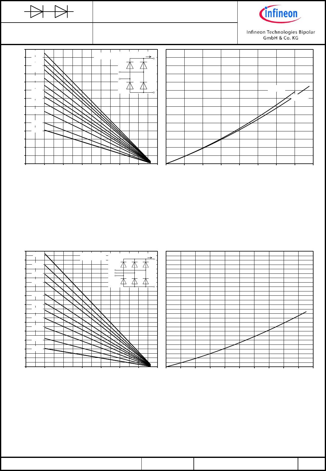
Durchlassverlustleistung je Zweig / On-state power loss per arm P
FAV
= f(I
FAV
)
Parameter: Stromflußwinkel / Current conduction angle
Θ
20
40
60
80
100
120
140
0
50
100
150
200
250
300
T
C
[°
C]
I
FAVM
[A
]
DC
Θ = 60
rec
120
rec
180
rec
180
sin
Höchstzulässige Gehäusetemperatur / Maximum allowable case temperature T
C
= f(I
FAVM
)
Strombelastung je Zweig / Current load per arm
Berechungsgrundlage P
TAV
Calculation base P
TAV
Parameter: Stromflußwinkel
Θ
/ Current conduction angle
Θ
Netz-Dioden-M
odul
Rectifier Diode M
odule
Technische Informati
on
/
technical information
DD180N
16S
Date of Publication 2017-
08
-
24
Revision 3
.3
8/
10
Seite/page
0,005
0,010
0,020
0,030
0,040
0,050
0,060
0,075
0,100
0,150
0,200
0,015
0,200
0,200
0
100
200
300
400
500
600
700
800
900
1000
1100
1200
1300
1400
0
20
40
60
80
100
120
140
P
tot
[W]
T
A
[°
C]
+
-
B2
I
D
~
R
thCA
[
K/W]
0
50
100
150
200
250
300
350
400
I
D
[A]
L-Last
R-Last
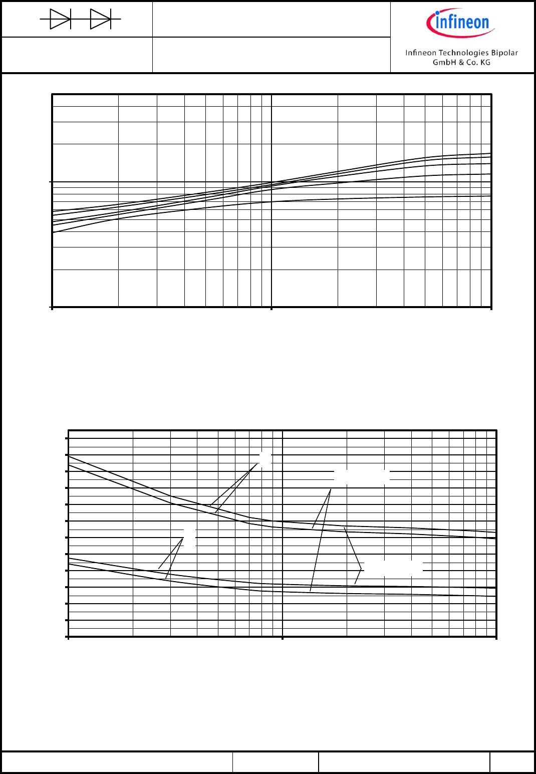
Höchstzulässiger Ausgangsstrom / Maximum rated outp
ut current I
D
B2
- Zweipuls-Brückenschaltung / Two-pulse bridge circuit
Gesamtverlustleistung der Schaltung / Total power dissipatio
n at circuit P
tot
Parameter:
W
är
mewiderstand zwischen den Gehäusen und Umgebung / Thermal resistance cases to
ambient R
thCA
0,015
0,020
0,025
0,030
0,040
0,050
0,060
0,075
0,100
0,150
0,250
0,250
0,250
0
200
400
600
800
1000
1200
1400
1600
1800
2000
2200
2400
2600
0
20
40
60
80
100
120
140
P
tot
[W]
T
A
[°
C]
+
-
B6
I
D
3~
R
thCA
[
K/W]
0,25
0
50
100
150
200
250
300
350
400
450
500
I
D
[A]
Höchstzulässiger Ausgangsstrom / Maximum rated outp
ut current I
D
B6
- Sechspuls-Brückenschaltung / Six-pulse bridge circuit
Gesamtverlustleistung der Schaltung / Total power dissipation at circuit P
tot
Parameter:
W
är
mewiderstand zwischen den Gehäusen und Umgebung
/ Thermal resistance cases to ambient R
thCA
Netz-Dioden-M
odul
Rectifier Diode M
odule
Technische Informati
on
/
technical information
DD180N
16S
Date of Publication 2017-
08
-
24
Revision 3
.3
9/
10
Seite/page
100
1000
1
10
100
Q
r
[µAs]
-di/dt [A
/µs]
i
TM
=
1000A
500A
200A
100A
50A
Sperrverzögerungsladung / Recovered charge Q
r
= f(-di/dt)
T
vj
= T
vjmax
, v
R
≤ 0,5 V
RRM
, v
RM
= 0,8 V
RRM
Parameter: Durchlaßstrom / On-state current i
FM
0
200
400
600
800
1.000
1.200
1.400
1.600
1.800
2.000
2.200
2.400
0,01
0,1
1
I
F(OV)M
[A
]
t [s]
a
T
A
= 35
C
b
T
A
= 45
C
Grenzstrom je Zweig / Maximum overload on-state current per arm I
F(OV)M
= f(t), v
RM
= 0,8 V
RRM
a: Leerlauf / No-load conditions
b: Vorlaststrom je Zweig / Pre-load current per arm I
FAV(vor)
= I
FAVM
T
a
= 35°C, verstärkte Luftkühlung / Forced air cooling Kühlkörper / Heatsink type:
KM17 (
Papst 4650)
T
a
= 45°C, natürliche Luftkühlung / Natural air cooling Kühlkörper / Heatsink type:
KM
17 (60W)
P1-P3
P4-P6
P7-P9
P10-P10
DD180N16SHPSA1
Mfr. #:
Buy DD180N16SHPSA1
Manufacturer:
Infineon Technologies
Description:
Discrete Semiconductor Modules Solder Contact Modules
Lifecycle:
New from this manufacturer.
Delivery:
DHL
FedEx
Ups
TNT
EMS
Payment:
T/T
Paypal
Visa
MoneyGram
Western
Union
Products related to this Datasheet
DD180N16SHPSA1