DATASHEET
9ZXL1231 REVISION J 05/25/16 1 ©2016 Integrated Device Technology, Inc.
12-output DB1200ZL 9ZXL1231
General Description
The 9ZXL1231 meets the demanding requirements of the
Intel DB1200ZL specification, including the critical low-drift
requirements of Intel CPUs.
Recommended Application
Buffer for Romley, Grantley and Purley Servers, solid state
storage and PCIe
Output Features
12 - Low-Power (LP) HCSL output pairs
Key Specifications
Cycle-to-cycle jitter <50ps
Output-to-output skew <50 ps
Input-to-output delay variation <50ps
PCIe Gen3 phase jitter <1.0ps RMS
Phase jitter: QPI/UPI >=9.6GB/s <0.2ps rms
Features/Benefits
Low-power push-pull HCSL outputs; eliminate 24 resistors,
save 41mm
2
of area
Pin compatible to 9ZX21201; easy path to >50% power
savings
Space-saving 64 VFQFPN package
Fixed feedback path for 0ps input-to-output delay
9 Selectable SMBus Addresses; multiple devices can
share the same SMBus Segment
12 OE# pins; hardware control of each output
PLL or bypass mode; PLL can dejitter incoming clock
Selectable PLL bandwidth; minimizes jitter peaking in
downstream PLL's
Spread Spectrum Compatible; tracks spreading input clock
for low EMI
Block Diagram
Logic
DIF(11:0)
HIBW_BYPM_LOBW#
SMBDAT
SMBCLK
CKPWRGD/PD#
SMB_A0_tri
SMB_A1_tri
100M_133M#
Z-PLL
(SS Compatible)
DFB_OUT_NC
DIF_IN
DIF_IN#
OE(11:0)#
12-OUTPUT DB1200ZL 2 REVISION J 05/25/16
9ZXL1231 DATASHEET
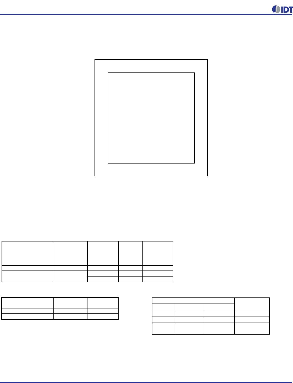
Pin Configuration
Power Management Table
Functionality at Power-up (PLL mode) Power Connections
DIF_11#
DIF_11
vOE11#
vOE10#
DIF_10#
DIF_10
GND
VDD
VDDIO
DIF_9#
DIF_9
vOE9#
vOE8#
DIF_8#
DIF_8
VDDIO
64 63 62 61 60 59 58 57 56 55 54 53 52 51 50 49
VDDA
148
GND
GNDA
247
DIF_7#
NC
346
DIF_7
100M_133M#
445
vOE 7#
HIBW_BYPM_LOBW#
544
vOE 6#
CKPWRGD_PD#
643
DIF_6#
GND
742
DIF_6
VDDR
841
GND
DIF_IN
940
VDD
DIF_IN#
10 39
DIF_5#
SMB_A0_tri
11 38
DIF_5
SMBDAT
12 37
vOE 5#
SMBCLK
13 36
vOE 4#
SMB_A1_tri
14 35
DIF_4#
DFB_OUT_NC#
15 34
DIF_4
DFB_OUT_NC
16 33
GND
17 18 19 20 21 22 23 24 25 26 27 28 29 30 31 32
DIF_0
DIF_0#
vOE0
#
vOE1
#
DIF_1
DIF_1#
GND
VDD
VDDIO
DIF_2
DIF_2#
vOE2
#
vOE3
#
DIF_3
DIF_3#
VDDIO
Note: Pins with ^ prefix have internal 120K pullup
Pins with v prefix have internal 120K pulldowm
9ZXL1231
connect epad to ground
9x9mm 64-pin VFQFPN
CKPWRGD_PD#
DIF_IN/
DIF_IN#
SMBus
EN bit
DIF(11:0)/
DIF(11:0)#
PLL STATE
IF NOT IN
BYPASS
MODE
0XXLow/LowOFF
0Low/LowON
1Runnin
g
ON
Running1
100M_133 M#
DIF_IN
MHz
DIF(11:0)
1 100.00 DIF_IN
0 133.33 DIF_IN
VDD VDDIO GND
12
Analo
g
PLL
8 7 Analog Input
24,40,57 25,32,49,56 23,33,41,48,58 DIF clocks
Pin Number
Description
REVISION J 05/25/16 3 12-OUTPUT DB1200ZL
9ZXL1231 DATASHEET
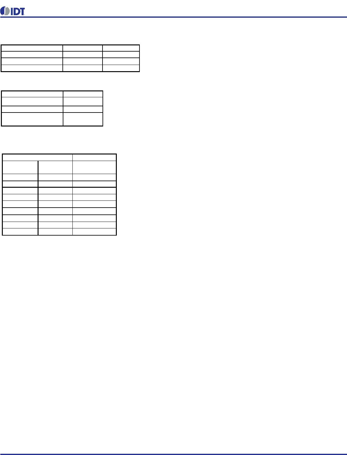
PLL Operating Mode Readback Table
PLL Operating Mode
9ZXL1231 SMBus Addressing
HiBW_BypM_LoBW# Byte0, bit 7 Byte 0, bit 6
Low (Low BW) 0 0
Mid (Bypass) 0 1
High (High BW) 1 1
HiBW_By pM_LoBW# MODE
Low PLL Lo BW
Mid Bypa ss
High PLL Hi BW
NOTE: PLL is OFF in Bypass Mode
SMB_A1_tri SMB_A0_tri
SMBus Address
0
0
D8
0
M
DA
01 DE
M
0
C2
M
M
C4
M1 C6
10 CA
1M CC
1
1
CE
Pin

9ZXL1231AKLFT

Mfr. #:
Manufacturer:
IDT
Description:
Clock Buffer HIGH PERF. ZDB - LOW POWER
Lifecycle:
New from this manufacturer.
Delivery:
DHL FedEx Ups TNT EMS
Payment:
T/T Paypal Visa MoneyGram Western Union

Products related to this Datasheet