1
FN8230.4
ISL90462
Single Volatile 32-tap XDCP
Digitally Controlled Potentiometer
(XDCP™)
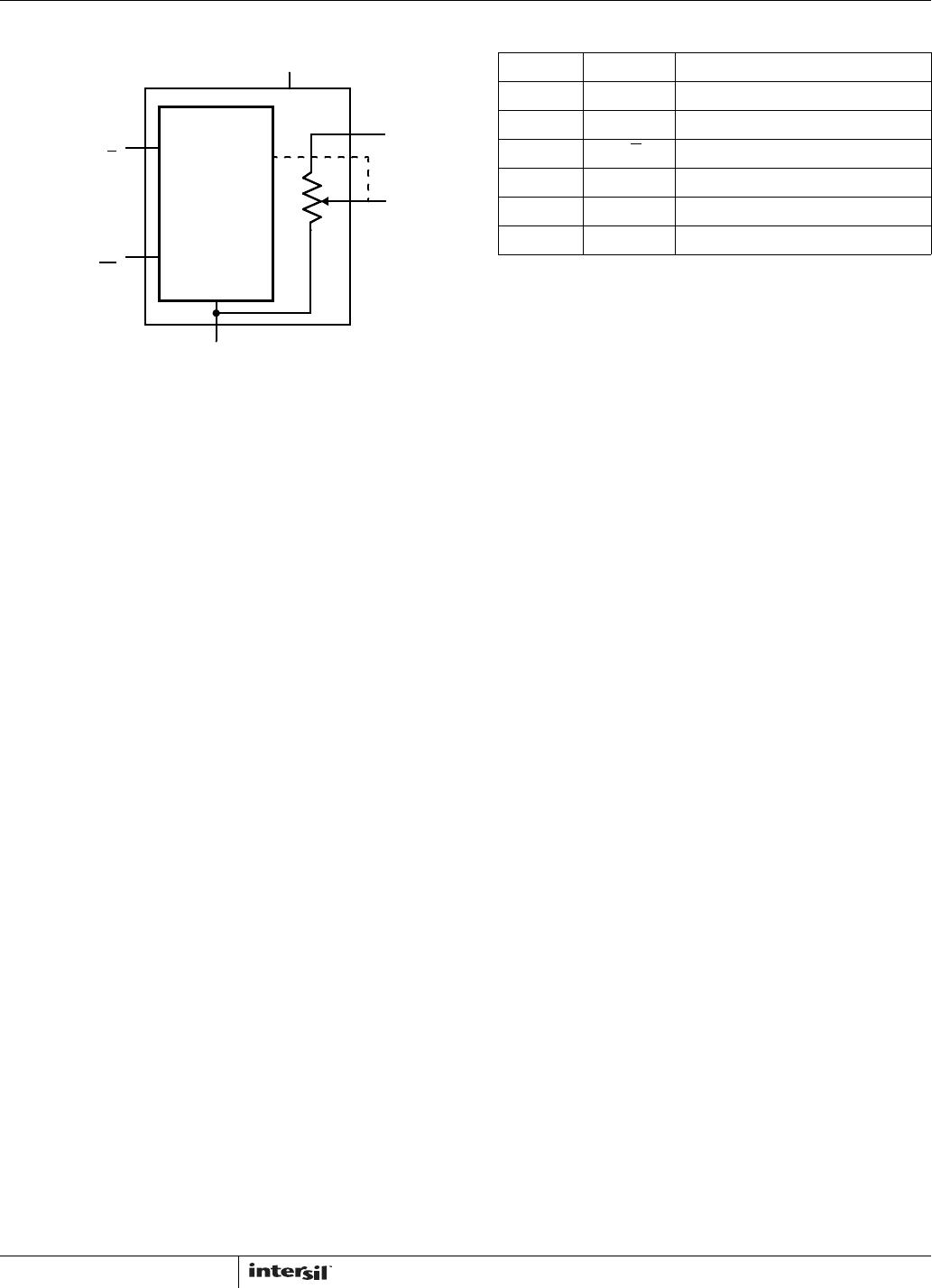
The Intersil ISL90462 is a digitally controlled potentiometer
(XDCP). Configured as a variable resistor, the device
consists of a resistor array, wiper switches, a control section,
and volatile memory. The wiper position is controlled by a 2-
pin Up /Down interface.
The potentiometer is implemented by a resistor array
composed of 31 resistive elements and a wiper switching
network. Between each element and at either end are tap
points accessible to the wiper terminal. The position of the
wiper element is controlled by the CS
and U/D inputs.
The device can be used in a wide variety of applications
including:
• LCD contrast control
• Parameter and bias adjustments
• Industrial and Automotive Control
• Transducer adjustment of pressure, temperature, position,
chemical, and optical sensors
• Laser Diode driver biasing
• Gain control and offset adjustment
Features
• Volatile Solid-State Potentiometer
• 2-pin UP/DN Interface
• DCP Terminal Voltage, 2.7V to 5.5V
• Tempco 35ppm/
°C Typical
• 32 Wiper Tap Points
• Low Power CMOS
- Active current, 25µA max.
- Supply current 0.3µA
• Available R
TOTAL
Values = 10k50k100k
• Temperature Range
-40°C to +85°C
• Packages
- 6 Ld SC-70, SOT-23
• Pb-Free Plus Anneal Available (RoHS Compliant)
Pinout
ISL90462
(SOT23, SC70)
TOP VIEW
Ordering Information
PART NUMBER PART MARKING R
TOTAL
(K) TEMP RANGE (°C) PACKAGE (Tape and Reel) PKG. DWG. #
ISL90462WIE627Z-TK (See Note) DEK 10 -40 to +85 6 Ld SC-70 (Pb-free) P6.049
ISL90462WIH627Z-TK (See Note) DEL -40 to +85 6 Ld SOT-23 (Pb-free) P6.064
ISL90462UIE627Z-TK (See Note) DEI 50 -40 to +85 6 Ld SC-70 (Pb-free) P6.049
ISL90462UIH627Z-TK (See Note) DEJ -40 to +85 6 Ld SOT-23 (Pb-free) P6.064
ISL90462TIE627Z-TK (See Note) DEG 100 -40 to +85 6 Ld SC-70 (Pb-free) P6.049
ISL90462TIH627Z-TK See Note)
(No longer available,
recommended replacement:I
SL90462UIE627Z-TK)
DEH -40 to +85 6 Ld SOT-23 (Pb-free) P6.064
NOTE: Intersil Pb-free plus anneal products employ special Pb-free material sets; molding compounds/die attach materials and 100% matte tin plate termination finish, which are
RoHS compliant and compatible with both SnPb and Pb-free soldering operations. Intersil Pb-free products are MSL classified at Pb-free peak reflow temperatures that meet or exceed
the Pb-free requirements of IPC/JEDEC J STD-020
Data Sheet October 20, 2015
CAUTION: These devices are sensitive to electrostatic discharge; follow proper IC Handling Procedures.
1-888-INTERSIL or 1-888-468-3774
| Copyright Intersil Americas LLC 2005, 2015. All Rights Reserved
XDCP and Intersil (and design) are trademarks owned by Intersil Corporation or one of its subsidiaries.
All other trademarks mentioned are the property of their respective owners.