TC4467/TC4468/TC4469
DS21425C-page 4 2001-2012 Microchip Technology Inc.
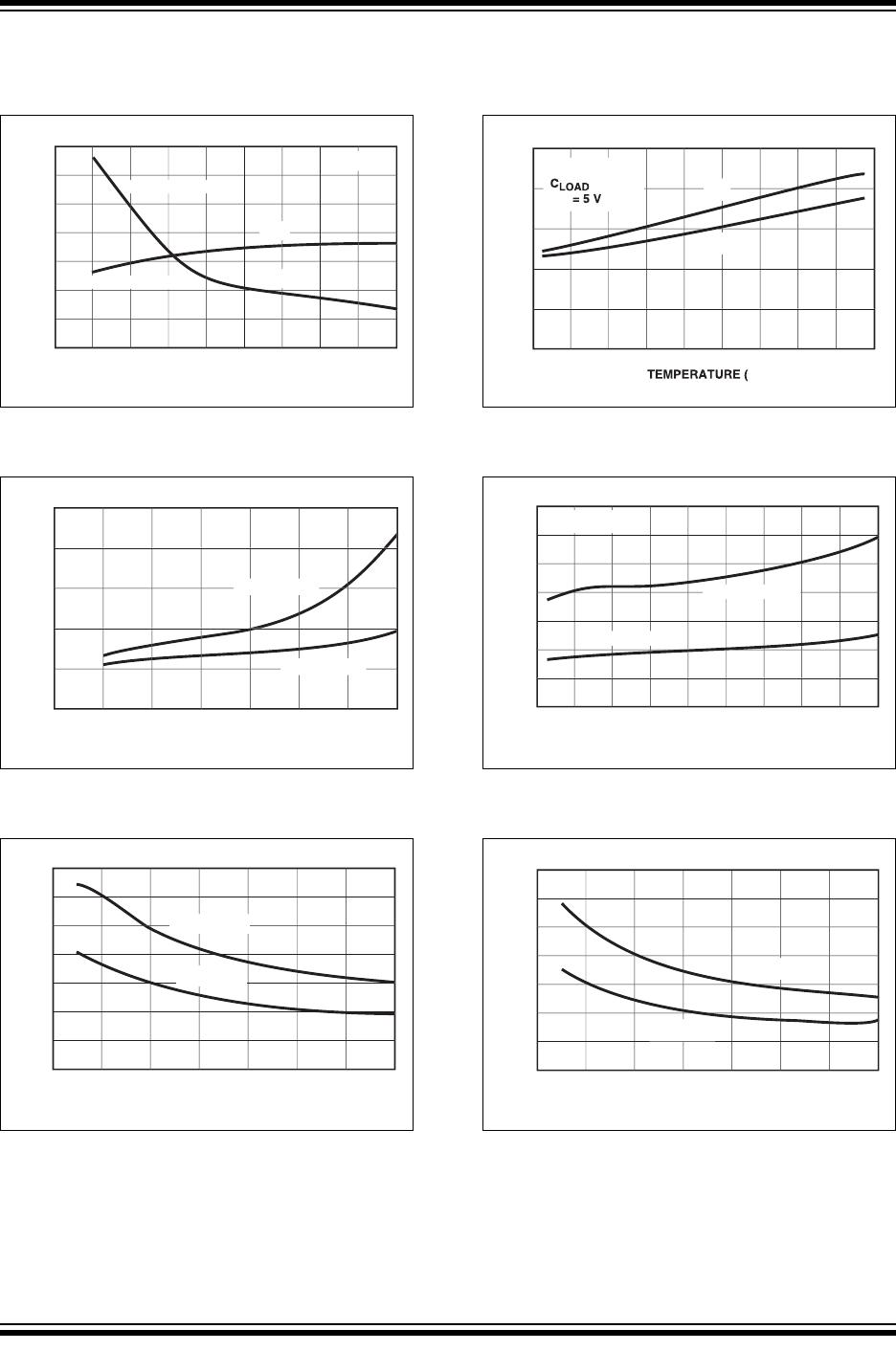
ELECTRICAL SPECIFICATIONS (OPERATING TEMPERATURES)
TRUTH TABLE
Electrical Characteristics: Unless otherwise noted, over operating temperature range with 4.5 V V
DD
18 V.
Parameters Sym Min Typ Max Units Conditions
Input
Logic 1, High Input Voltage V
IH
2.4 V Note 3
Logic 0, Low Input Voltage V
IL
——0.8VNote 3
Input Current I
IN
-10 10 µA 0 VV
IN
V
DD
Output
High Output Voltage V
OH
V
DD
– 0.025 V I
LOAD
= 100 µA (Note 1)
Low Output Voltage V
OL
0.30 V I
LOAD
= 10 mA (Note 1)
Output Resistance R
O
—2030 I
OUT
= 10 mA, V
DD
= 18 V
Peak Output Current I
PK
—1.2A
Continuous Output Current I
DC
300 mA Single Output
500 Total Package
Latch-Up Protection Withstand
Reverse Current
I 500 mA 4.5 VV
DD
16 V
Switching Time (Note 1)
Rise Time t
R
15 50 nsec Figure 4-1
Fall Time t
F
15 50 nsec Figure 4-1
Delay Time t
D1
40 100 nsec Figure 4-1
Delay Time t
D2
40 100 nsec Figure 4-1
Power Supply
Power Supply Current I
S
——8mA
Power Supply Voltage V
DD
4.5 18 V Note 2
Note 1: Totem pole outputs should not be paralleled because the propagation delay differences from one to the other could cause one driver to
drive high a few nanoseconds before another. The resulting current spike, although short, may decrease the life of the device. Switching
times are ensured by design.
2: When driving all four outputs simultaneously in the same direction, V
DD
will be limited to 16 V. This reduces the chance that internal dv/dt
will cause high-power dissipation in the device.
3: The input threshold has approximately 50 mV of hysteresis centered at approximately 1.5 V. Input rise times should be kept below 5 µsec
to avoid high internal peak currents during input transitions. Static input levels should also be maintained above the maximum, or below
the minimum, input levels specified in the "Electrical Characteristics" to avoid increased power dissipation in the device.
Part No. TC4467 NAND TC4468 AND TC4469 AND/INV
Inputs A HHLLHHLLHHLL
Inputs B HLHLHLHLHLHL
Outputs TC446XLHHHHLLLLHLL
Legend: H = High L = Low
2001-2012 Microchip Technology Inc. DS21425C-page 5
TC4467/TC4468/TC4469
2.0 TYPICAL PERFORMANCE CURVES
Note: T
A
= +25°C, with 4.5 V V
DD
18 V.
FIGURE 2-1: Rise Time vs. Supply
Voltage.
FIGURE 2-2: Rise Time vs. Capacitive
Load.
FIGURE 2-3: Rise/Fall Times vs.
Temperature.
FIGURE 2-4: Fall Time vs. Supply
Voltage.
FIGURE 2-5: Fall Time vs. Capacitive
Load.
FIGURE 2-6: Propagation Delay Time vs.
Supply Voltage.
Note: The graphs and tables provided following this note are a statistical summary based on a limited number of
samples and are provided for informational purposes only. The performance characteristics listed herein are
not tested or guaranteed. In some graphs or tables, the data presented may be outside the specified
operating range (e.g., outside specified power supply range) and therefore outside the warranted range.
14
0
12
0
1
00
80
60
4
0
2
0
0
5
7
9
11
1
3
1
5
17
1
9
2200 pF
0
p
p
1600
pF
1000
pF
470
pF
100
pF
t
R
I
S
E
(
nsec
)
V
SU
PPL
Y
(
V
)
14
0
12
0
1
00
80
60
4
0
2
0
0
1
00
1
000
10
,
00
0
10 V
15 V
V
V
V
5
V
t
R
I
S
E
(
nsec
)
C
L
O
A
D
(
pF
)
0
-
50
TIME
(
nsec
)
5
1
0
1
5
2
0
2
5
-2
5
0
2
5
50
7
5
1
00
12
5
t
FALL
t
RISE
V
SU
PPL
Y
= 17.
5
V
C
L
O
A
D
= 470
pF
TEMPERATURE
(
°
C
)
14
0
12
0
1
00
80
60
4
0
2
0
0
3
5
7
9
11
1
3
1
5
17
1
9
p
100
pF
470
pF
1000
pF
1500
pF
2200
pF
t
FALL
(
nsec
)
V
SU
PPL
Y
(V
)
14
0
12
0
1
00
80
60
4
0
2
0
0
100
0
0
1
000
10
,
00
0
V
V
V
5
V
10 V
15 V
t
FALL
(
nsec
)
C
L
O
A
D
(
pF
)
0
4
D
ELAY TIME
(
nsec
)
2
0
4
0
60
80
8
1
2
1
4
1
6
1
8
6
1
0
V
SU
PPL
Y
(
V
)
t
t
D1
t
D2
C
C
L
O
A
D
4
70
pF
=
4
TC4467/TC4468/TC4469
DS21425C-page 6 2001-2012 Microchip Technology Inc.
2.0 TYPICAL PERFORMANCE CURVES (CONTINUED)
Note: T
A
= +25°C, with 4.5 V V
DD
18 V.
FIGURE 2-7: Input Amplitude vs. Delay
Times.
FIGURE 2-8: Quiescent Supply Current
vs. Supply Voltage.
FIGURE 2-9: High-State Output
Resistance.
FIGURE 2-10: Propagation Delay Times
vs. Temperatures.
FIGURE 2-11: Quiescent Supply Current
vs. Temperature.
FIGURE 2-12: Low-State Output
Resistance.
14
0
12
0
1
00
80
60
4
0
2
0
0
1
9
1
0
D
ELAY TIME
(
nsec
)
2
3
4
5
6
7
8
INP
U
T FALLIN
G
INP
U
T RI
S
IN
G
V
DRIVE
(
V
)
t
D1
t
D2
V
DD
V
=
12 V
0
4
0
.
5
1.
0
1.
5
2.
0
2.
5
6
8
1
0
12
14
1
6
1
8
OU
TP
U
T
S
=
1
OUTPUTS = 0
V
SU
PPL
Y
(V
)
I
Q
UIESCENT
(
mA
)
0
4
6
8
1
0
12
14
1
6
1
8
V
SU
PPL
Y
(
V
)
5
1
0
1
5
2
0
2
5
30
35
R
D
S
(
ON
)
(
Ω
)
T
J
= +1
50
°
C
T
J
= +25°C
7
0
2
0
1
00
12
0
D
ELAY TIME
(
nsec
)
-4
0
-2
0
0
2
0
4
0
60
80
30
4
0
50
60
-
60
°
C
)
V
DD
= 17.
5
V
= 470
pF
V
IN
t
D1
t
D2
3
.
5
0
1
00
12
0
-4
0
-2
0
0
2
0
4
0
60
80
3
.
0
2.
5
2.
0
1.
5
1.
0
0
.
5
OU
TP
U
T
S
=
1
OUTPUTS = 0
-
60
I
Q
UIESCENT
(mA)
T
J
U
N
C
TI
ON
(
°
C
)
V
V
DD
= 17.
5
V
0
4
6
8
1
0
1
2
1
4
1
6
1
8
5
1
0
1
5
2
0
2
5
30
35
V
SU
PPLY
(
V
)
R
D
S
(
ON
)
(
Ω
)
T
J
= +150
°
C
T
J
= +2
5
°
C

TC4469COE713

Mfr. #:
Manufacturer:
Microchip Technology
Description:
Gate Drivers 1.2A Quad LOGIC I/P
Lifecycle:
New from this manufacturer.
Delivery:
DHL FedEx Ups TNT EMS
Payment:
T/T Paypal Visa MoneyGram Western Union