MAX5166
32-Channel Sample/Hold Amplifier
with Four Multiplexed Inputs
2 _______________________________________________________________________________________
ABSOLUTE MAXIMUM RATINGS
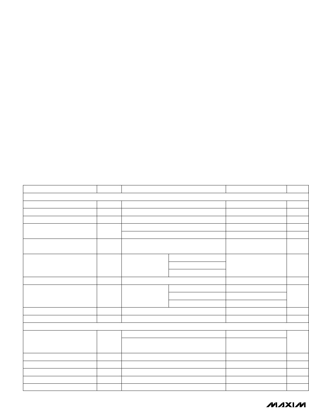
ELECTRICAL CHARACTERISTICS
(V
DD
= +10V, V
SS
= -5V, V
L
= +5V ±5%, AGND = DGND, R
L
= 5kΩ, C
L
= 50pF, T
A
= T
MIN
to T
MAX
, unless otherwise noted. Typical
values are at T
A
= +25°C.)
Stresses beyond those listed under “Absolute Maximum Ratings” may cause permanent damage to the device. These are stress ratings only, and functional
operation of the device at these or any other conditions beyond those indicated in the operational sections of the specifications is not implied. Exposure to
absolute maximum rating conditions for extended periods may affect device reliability.
V
DD
to AGND.......................................................-0.3V to +11.0V
V
SS
to AGND .........................................................-6.0V to +0.3V
V
DD
to V
SS
......................................................................+15.75V
V
L
to DGND ...........................................................-0.3V to +6.0V
V
L
to AGND ...........................................................-0.3V to +6.0V
DGND to AGND.....................................................-0.3V to +2.0V
IN_ to AGND ...............................................................V
SS
to V
DD
A_, M_ to DGND ....................................................-0.3V to +6.0V
Maximum Current into Output Pin ....................................±10mA
Maximum Current into A_, M_ ..........................................±20mA
Continuous Power Dissipation (T
A
= +70°C)
48-Pin TQFP (derate 12.5mW/°C above +70°C)..................1W
Operating Temperature Ranges
MAX5166_CCM ...................................................0°C to +70°C
MAX5166_ECM.................................................-40°C to +85°C
Storage Temperature Range .............................-65°C to +150°C
Lead Temperature (soldering, 10sec) .............................+300°C
Figure 2 (Note 1)
Figure 2 (Note 1)
Figure 2 (Note 1)
IN_ = AGND
To ±1mV of final value, Figure 2 (Note 1)
-4V < V
IN
< +7V, R
L
= ∞
T
A
= +25°C, 100mV step to ±1mV, R
L
= ∞,
Figure 2 (Note 2)
8V step to 0.08%, R
L
= ∞, Figure 2 (Note 2)
(Note 1)
IN_ = AGND, T
A
= +25°C
IN_ = AGND, T
A
= +25°C
+15°C ≤ T
A
≤ +65°C (Note 1)
R
L
= ∞,
C
L
= 250pF
CONDITIONS
ns150t
DH
Data Hold Time
ns200t
PW
Inhibit Pulse Width
ns200t
AP
Aperture Delay
µs12t
H
Hold-Mode Settling Time
µs
1
t
AQ
2.5 4
Acquisition Time
mA2I
SINK
Output Sink Current
mA2I
SOURCE
Output Source Current
Ω
700 1000 1300
R
OUT_
DC Output Impedance
mV0.25 1.00V
HS
Hold Step
%0.01 0.08Linearity Error
350 500 650
35 50 65
pF520C
IN_
Input Capacitance
mV/sec140
∆
V
OUT
Droop Rate
mV-30 -5 +30
µV/°C20 40
V
OS
Offset Voltage
UNITSMIN TYP MAXSYMBOLPARAMETER
8V step with
500ns rising edge
(Note 1)
Analog Crosstalk
MAX5166L
MAX5166M
MAX5166N
R
L
= ∞
V
V
SS
+ V
DD
-
0.75 2.4
V
OUT_
Output Voltage Range
MAX5165M, C
L
= 10nF
MAX5165N, C
L
= 10nF
MAX5165L, C
L
= 250pF
Figure 2 (Note 1) ns50t
DS
Data Setup Time
ANALOG SECTION
TIMING PERFORMANCE
dB-72 -76