Hold Step
When switching between sample mode and hold
mode, the voltage of the hold capacitor changes due to
charge injection from stray capacitance. This voltage
change, called hold step, is minimized by limiting the
amount of stray capacitance seen by the hold capaci-
tor. The MAX5166 limits the hold step to 0.25mV (typ).
An output capacitor to ground can be used to filter out
this small hold-step error.
Output
The MAX5166 contains an output buffer for each multi-
plexer channel (32 total), so the hold capacitor sees a
high-impedance input, reducing the droop rate. While
in hold mode, the hold capacitor discharges at a rate of
1mV/sec (typ). The buffer also provides a low output
impedance; however, the device contains output resis-
tors in series with the buffer output (Figure 1) for select-
ed output filtering. To provide greater design flexibility,
the MAX5166 is available with an R
O
of 50Ω, 500Ω, or
1kΩ.
Note: Output loads increase the analog supply cur-
rent (I
DD
and I
SS
). Excessive loading of the output(s)
damages the device by consuming more power than
the device will dissipate (see Absolute Maximum
Ratings). The resistor-divider formed by the output
resistor (R
OUT_
) and load impedance (R
L
) scales the
sampled voltage (V
SAMP
). Determine the output volt-
age (V
OUT_
) as follows:
Voltage Gain = A
V
= R
L
/(R
L
+ R
OUT
)
V
OUT_
= V
SAMP
· A
V
The maximum output voltage range depends on the
analog supply voltages available and the scaling factor
used:
(V
SS
+ 0.75V) · A
V
≤ V
OUT_
≤ (V
DD
- 2.4V) · A
V
when R
L
= ∞, then A
V
= 1, and this equation becomes
(V
SS
+ 0.75V) ≤ V
OUT
≤ (V
DD
- 2.4V).
Timing Definitions
Acquisition time (t
AQ
) is the amount of time the
MAX5166 must remain in sample mode for the hold
capacitor to acquire an accurate sample. The hold-
mode settling time (t
H
) is the amount of time necessary
for the output voltage to settle to its final value.
Aperture delay (t
AP
) is the time interval required to dis-
connect the input from the hold capacitor. The inhibit
pulse width (t
PW
) is the amount of time the MAX5166
must remain in hold mode while the address is
changed. The data setup time (t
DS
) is the amount of
time an address must be maintained before the
address becomes valid. The data hold time (t
DH
) is the
amount of time an address must be maintained after
mode select has gone from low to high (Figure 2).
MAX5166
32-Channel Sample/Hold Amplifier
with Four Multiplexed Inputs
_______________________________________________________________________________________ 7
0
0
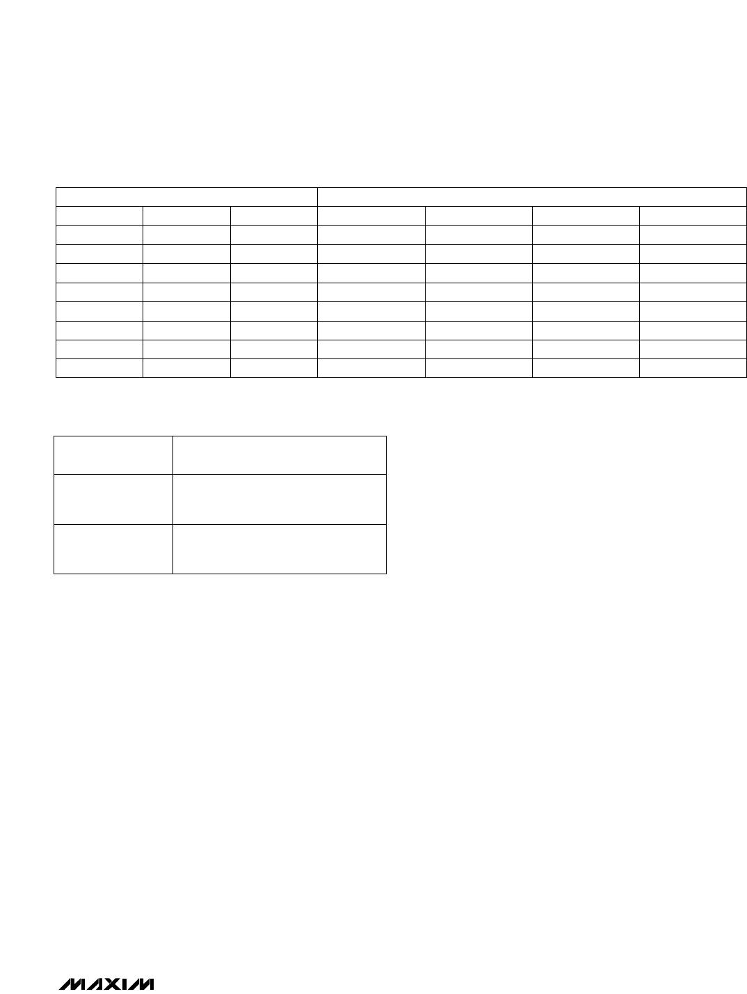
Table 1. Output Selection
Table 2. Mode Selection
0
0
1
1
1
1
1
1
1
1
0
0
0
0
0
1
0
1
ADDRESS
0
1
0
1
OUT2
OUT3
OUT6
OUT0
OUT7
OUT1
OUT4
OUT5
OUT10
OUT11
OUT14
OUT8
OUT15
OUT9
OUT12
OUT13
OUT18
OUT19
OUT22
OUT16
OUT23
OUT17
OUT20
OUT21
OUTPUT SELECTED
OUT26
OUT27
OUT30
OUT24
OUT31
OUT25
OUT28
OUT29
A2 A1 A0 MUX0 MUX1 MUX2 MUX3
0 = Logic Low, 1 = Logic High
0
1
Sample mode enabled on selected
analog multiplexer and channel
(Table 1).
Hold mode enabled on selected
analog multiplexer and channel
(Table 1).
MODE-SELECT
INPUTS* (M3–M0)
ACTION
0 = Logic Low, 1 = Logic High
* Only one M_ input asserted low; all others must be logic high
to meet the timing specification (see Single vs. Simultaneous
Sampling).