Nexperia
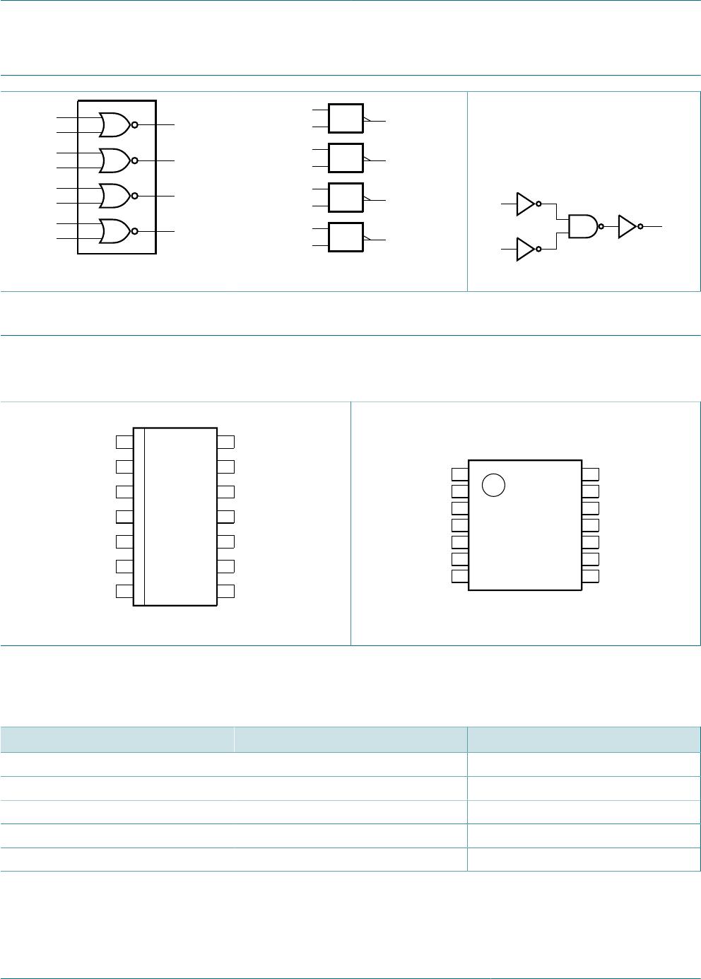
74LVT02
3.3 V Quad 2-input NOR gate
74LVT02 All information provided in this document is subject to legal disclaimers. © Nexperia B.V. 2017. All rights reserved.
Product data sheet Rev. 3 — 7 April 2017
3 / 13
6 Functional description
Table 3. Function table
[1]
Input Output
nA nB nY
L L H
L H L
H L L
H H L
[1] H = HIGH voltage level; L = LOW voltage level
7 Limiting values
Table 4. Limiting values
In accordance with the Absolute Maximum Rating System (IEC 60134). Voltages are referenced to GND (ground = 0 V).
Symbol Parameter Conditions Min Max Unit
V
CC
supply voltage -0.5 +4.6 V
V
I
input voltage
[1]
-0.5 +7.0 V
V
O
output voltage output in OFF-state or HIGH-state
[1]
-0.5 +7.0 V
I
IK
input clamping current V
I
< 0 V -50 - mA
I
OK
output clamping current V
O
< 0 V -50 - mA
output in LOW-state - 64 mAI
O
output current
output in HIGH-state -32 - mA
T
stg
storage temperature -65 +150 °C
T
j
junction temperature
[2]
- 150 °C
P
tot
total power dissipation T
amb
= -40 to +85 °C
[3]
- 500 mW
[1] The input and output negative voltage ratings may be exceeded if the input and output clamp current ratings are observed.
[2] The performance capability of a high-performance integrated circuit in conjunction with its thermal environment can create junction temperatures which
are detrimental to reliability.
[3] For SO14 packages: above 70 °C derate linearly with 8 mW/K.
For SSOP14 and TSSOP14 packages: above 60 °C derate linearly with 5.5 mW/K.
8 Recommended operating conditions
Table 5. Operating conditions
Symbol Parameter Conditions Min Typ Max Unit
V
CC
supply voltage 2.7 - 3.6 V
V
I
input voltage 0 - 5.5 V
I
OH
HIGH-level output current -20 - - mA
I
OL
LOW-level output current - - 32 mA
T
amb
ambient temperature in free-air -40 - +85 °C
Δt/ΔV input transition rise and fall rate outputs enabled - - 10 ns/V