Nexperia
74LVT02
3.3 V Quad 2-input NOR gate
74LVT02 All information provided in this document is subject to legal disclaimers. © Nexperia B.V. 2017. All rights reserved.
Product data sheet Rev. 3 — 7 April 2017
5 / 13
10 Dynamic characteristics
Table 7. Dynamic characteristics
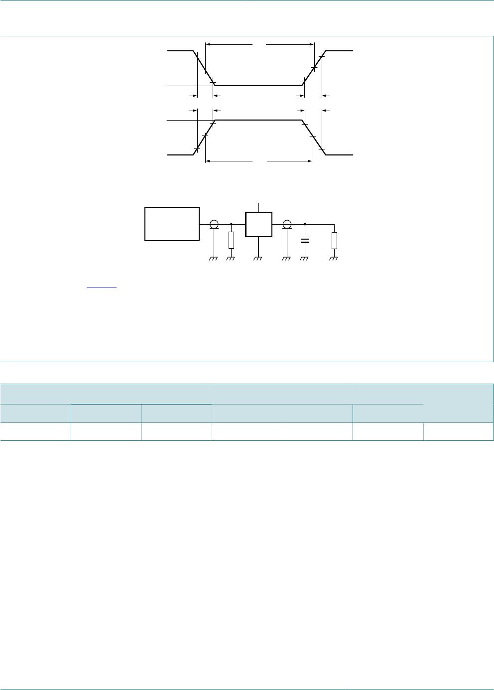
Voltages are referenced to GND (ground = 0 V); for test circuit see Figure 7.
Symbol Parameter Conditions Min Typ
[1]
Max Unit
T
amb
= -40 °C to +85 °C
nA or nB to nY; see Figure 6
V
CC
= 2.7 V - - 5.2 ns
t
PLH
LOW to HIGH
propagation delay
V
CC
= 3.0 V to 3.6 V 1 2.8 4.4 ns
nA or nB to nY; see Figure 6
V
CC
= 2.7 V - - 3.4 ns
t
PHL
HIGH to LOW
propagation delay
V
CC
= 3.0 V to 3.6 V 1 2.6 3.6 ns
[1] Typical values are measured at T
amb
= 25 °C and V
CC
= 3.3 V.
10.1 Waveforms and test circuit
mna612
t
PHL
t
PLH
V
M
V
M
A, B input
Y output
GND
V
I
V
OH
V
OL
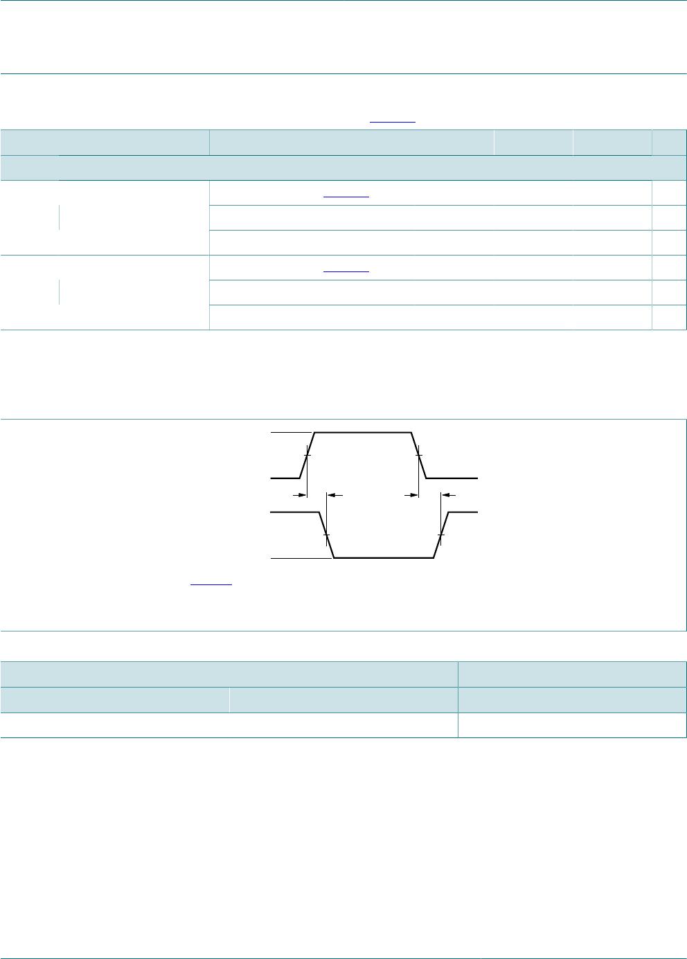
Measurement points are given in Table 8.
V
OL
and V
OH
are typical voltage output levels that occur with the output load.
Figure 6. Input to output propagation delays
Table 8. Measurement points
Input Output
V
M
V
I
V
M
1.5 V 2.7 V 1.5 V