XC18V00 Series In-System Programmable Configuration PROMs
20 www.xilinx.com DS026 (v4.1) December 15, 2003
1-800-255-7778 Product Specification
R
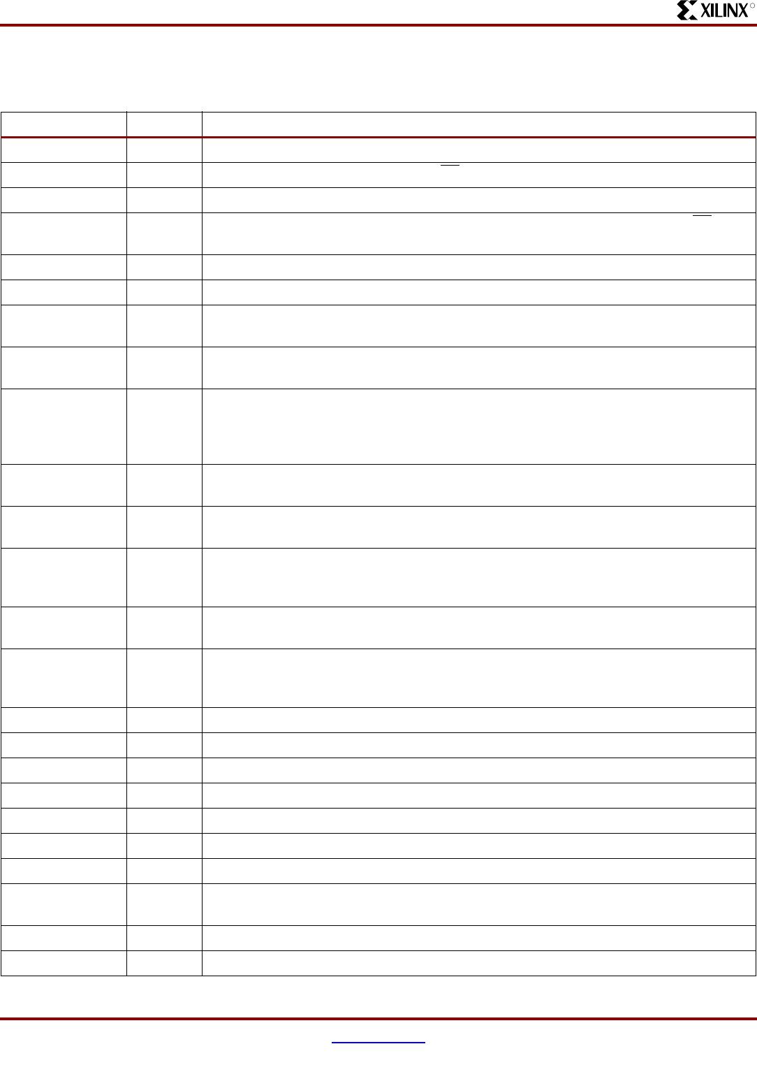
Revision History
The following table shows the revision history for this document.
Date Version Revision
2/9/99 1.0 First publication of this early access specification
8/23/99 1.1 Edited text, changed marking, added CF
and parallel load
9/1/99 1.2 Corrected JTAG order, Security and Endurance data.
9/16/99 1.3 Corrected SelectMAP diagram, control inputs, reset polarity. Added JTAG and CF
description, 256 Kbit and 128 Kbit devices.
01/20/00 2.0 Added Q44 Package, changed XC18xx to XC18Vxx
02/18/00 2.1 Updated JTAG configuration, AC and DC characteristics
04/04/00 2.2 Removed stand alone resistor on INIT pin in Figure 5. Added Virtex-E and EM parts to
FPGA table.
06/29/00 2.3 Removed XC18V128 and updated format. Added AC characteristics for XC18V01,
XC18V512, and XC18V256 densities.
11/13/00 2.4 Features: changed 264 MHz to 264 Mb/s at 33 MHz; AC Spec.: T
SCE
units to ns, T
HCE
CE High time units to µs. Removed Standby Mode statement: “The lower power standby
modes available on some XC18V00 devices are set by the user in the programming
software”. Changed 10,000 cycles endurance to 20,000 cycles.
01/15/01 2.5 Updated Figures 5 and 6, added 4.7 resistors. Identification registers: changes ISP
PROM product ID from 06h to 26h.
04/04/01 2.6 Updated Figure 6, Virtex SelectMAP mode; added XC2V products to Compatible PROM
table; changed Endurance from 10,000 cycles, 10 years to 20,000, 20 years;
04/30/01 2.7 Updated Figure 6: removed Virtex-E in Note 2, fixed SelectMAP mode connections.
Under AC Characteristics Over Operating Conditions for XC18V04 and XC18V02,
changed T
SCE
from 25 ms to 25 ns.
06/11/01 2.8 AC Characteristics Over Operating Conditions for XC18V01 and XC18V512.
Changed Min values for T
SCE
from 20 ms to 20 ns and for T
HCE
from 2 ms to 2 µs.
09/28/01 2.9 Changed the boundary scan order for the CEO pin in Table 1, updated the configuration
bits values in the table under Xilinx FPGAs and Compatible PROMs, and added
information to the Recommended Operating Conditions table.
11/12/01 3.0 Updated for Spartan-IIE FPGA family.
12/06/01 3.1 Changed Figure 7(c).
02/27/02 3.2 Updated Table 2 and Figure 6 for the Virtex-II Pro family of devices.
03/15/02 3.3 Updated Xilinx software and modified Figure 6 and Figure 7.
03/27/02 3.4 Made changes to pages 1-3, 5, 7-11, 13, 14, and 18. Added new Figure 8 and Figure 9.
06/14/02 3.5 Made additions and changes to Table 2.
07/24/02 3.6 Changed last bullet under Connecting Configuration PROMs, page 9.
09/06/02 3.7 Multiple minor changes throughout, plus the addition of Pinout Diagrams, page 4 and
the deletion of Figure 9.
10/31/02 3.8 Made minor change on Figure 7 (b) and changed orientation of SO20 diagram on page 5.
11/18/02 3.9 Added XC2S400E and XC2S600E to Table 2.