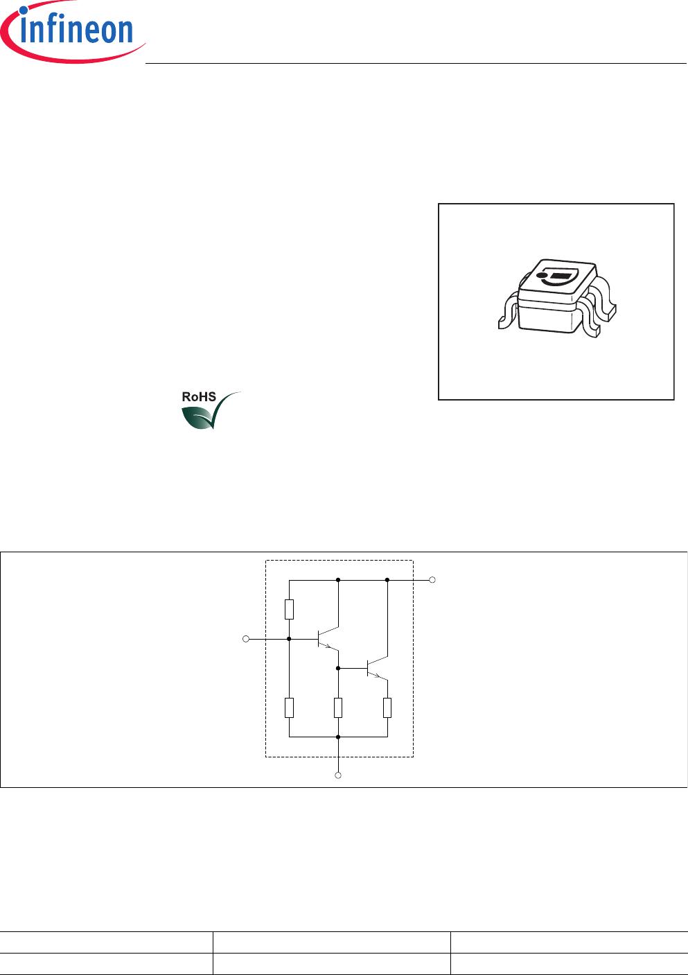
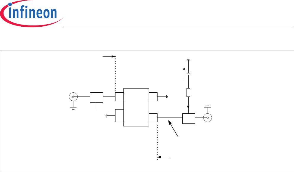
BGA614
Electrical Characteristics
Data Sheet 5 Rev. 2.1, 2011-09-02
Maximum Ratings
Note: All Voltages refer to GND-Node
Thermal resistance
2 Electrical Characteristics
Electrical characteristics at T
A
= 25 °C (measured in test circuit specified in Figure 2)
V
CC
= 5 V, R
Bias
= 62 Ω, Frequency = 2 GHz, unless otherwise specified
Table 1 Maximum ratings
Parameter Symbol Limit Value Unit
Device voltage
V
D
3V
Device current
I
D
80 mA
Current into pin In
I
in
0.7 mA
Input power
1)
1)Valid for Z
S
= Z
L
= 50 Ω, V
CC
= 5 V, R
Bias
= 62 Ω
P
in
10 dBm
Total power dissipation,
T
S
< 102 °C
2)
2) T
S
is measured on the ground lead at the soldering point
P
tot
240 mW
Junction temperature
T
J
150 °C
Ambient temperature range
T
A
-65... 150 °C
Storage temperature range
T
STG
-65... 150 °C
ESD capability all pins (HBM: JESD22-A114) V
ESD
1000 V
Table 2 Thermal resistance
Parameter Symbol Value Unit
Junction - soldering point
1)
1) For calculation of R
thJA
please refer to Application Note Thermal Resistance
R
thJS
200 K/W
Table 3 Electrical Characteristics
Parameter Symbol Values Unit Note /
Test Condition
Min. Typ. Max.
Insertion power gain
|S
21
|
2
19.8 dB f = 0.1 GHz
19.0 dB
f = 1.0 GHz
17.5 dB
f = 2.0 GHz
Noise figure (
Z
S
= 50 Ω) F
50Ω
1.8 dB f = 0.1 GHz
2.0 dB
f = 1.0 GHz
2.1 dB
f = 2.0 GHz
Output power at 1 dB gain
compression
P
-1dB
12 dBm
Output third order intercept point
OIP
3
25 dBm
Input return loss
RL
in
18 dB
Output return loss
RL
out
20 dB
Total device current
I
D
40 mA