AD629
Rev. C | Page 11 of 16
APPLICATIONS
BASIC CONNECTIONS
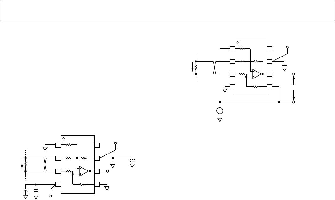
Figure 32 shows the basic connections for operating the AD629
with a dual supply. A supply voltage of between ±3 V and ±18 V
is applied between Pin 7 and Pin 4. Both supplies should be
decoupled close to the pins using 0.1 µF capacitors. Electrolytic
capacitors of 10 µF, also located close to the supply pins, may be
required if low frequency noise is present on the power supply.
While multiple amplifiers can be decoupled by a single set of
10 µF capacitors, each in amp should have its own set of 0.1 µF
capacitors so that the decoupling point can be located right at
the IC’s power pins.
REF (–)
REF (+)
–V
S
–V
S
+
S
+V
S
V
OUT
= I
SHUNT
× R
SHUNT
NC
–IN
+IN
R
SHUNT
I
SHUNT
(SEE
TEXT)
(SEE
TEXT)
0.1µF
0.1µF
+3V TO +18V
–3V TO –18V
NC = NO CONNECT
21.1kΩ
380kΩ 380kΩ
20kΩ
380kΩ
AD629
1
2
3
4
8
7
6
5
00783-030
Figure 32. Basic Connections
The differential input signal, which typically results from a load
current flowing through a small shunt resistor, is applied to
Pin 2 and Pin 3 with the polarity shown to obtain a positive
gain. The common-mode range on the differential input signal
can range from −270 V to +270 V, and the maximum differential
range is ±13 V. When configured as shown in Figure 32, the
device operates as a simple gain-of-1, differential-to-single-
ended amplifier; the output voltage being the shunt resistance
times the shunt current. The output is measured with respect to
Pin 1 and Pin 5.
Pin 1 and Pin 5 (REF(–) and REF(+)) should be grounded for a
gain of unity and should be connected to the same low impedance
ground plane. Failure to do this results in degraded common-
mode rejection. Pin 8 is a no connect pin and should be left open.
SINGLE-SUPPLY OPERATION
Figure 33 shows the connections for operating the AD629 with
a single supply. Because the output can swing to within only
about 2 V of either rail, it is necessary to apply an offset to the
output. This can be conveniently done by connecting REF(+)
and REF(–) to a low impedance reference voltage (some ADCs
provide this voltage as an output), which is capable of sinking
current. Therefore, for a single supply of 10 V, V
REF
may be set
to 5 V for a bipolar input signal. This allows the output to swing
±3 V around the central 5 V reference voltage. Alternatively, for
unipolar input signals, V
REF
can be set to about 2 V, allowing the
output to swing from 2 V (for a 0 V input) to within 2 V of the
positive rail.
REF (–)
REF (+)
–V
S
V
Y
V
X
+V
S
+V
S
NC
–IN
+IN
R
SHUNT
I
SHUNT
0.1µF
NC = NO CONNECT
21.1kΩ
380kΩ 380kΩ
20kΩ
380kΩ
AD629
1
2
3
4
8
7
6
5
00783-031
OUTPUT = V
OUT
– V
REF
V
REF
Figure 33. Operation with a Single Supply
Applying a reference voltage to REF(+) and REF(–) and
operating on a single supply reduces the input common-mode
range of the AD629. The new input common-mode range
depends upon the voltage at the inverting and noninverting
inputs of the internal operational amplifier, labeled V
X
and V
Y
in Figure 33. These nodes can swing to within 1 V of either rail.
Therefore, for a (single) supply voltage of 10 V, V
X
and V
Y
can
range between 1 V and 9 V. If V
REF
is set to 5 V, the permissible
common-mode range is +85 V to –75 V. The common-mode
voltage ranges can be calculated by
V
CM
(±) = 20 V
X
/V
Y
(±) − 19 V
REF
SYSTEM-LEVEL DECOUPLING AND GROUNDING
The use of ground planes is recommended to minimize the
impedance of ground returns (and therefore the size of dc
errors). Figure 34 shows how to work with grounding in a
mixed-signal environment, that is, with digital and analog
signals present. To isolate low level analog signals from a noisy
digital environment, many data acquisition components have
separate analog and digital ground returns. All ground pins
from mixed-signal components, such as ADCs, should return
through a low impedance analog ground plane. Digital ground
lines of mixed-signal converters should also be connected to the
analog ground plane. Typically, analog and digital grounds
should be separated; however, it is also a requirement to
minimize the voltage difference between digital and analog
grounds on a converter, to keep them as small as possible
(typically <0.3 V). The increased noise, caused by the
converter’s digital return currents flowing through the analog
ground plane, is typically negligible. Maximum isolation
between analog and digital is achieved by connecting the ground
planes back at the supplies. Note that Figure 34 suggests a “star”
ground system for the analog circuitry, with all ground lines
being connected, in this case, to the ADC’s analog ground.
However, when ground planes are used, it is sufficient to
connect ground pins to the nearest point on the low impedance
ground plane.

