AD629
Rev. C | Page 3 of 16
SPECIFICATIONS
T
A
= 25°C, V
S
= ±15 V, unless otherwise noted.
Table 1.
AD629A
1
AD629B
Parameter Condition Min Typ Max Min Typ Max Unit
GAIN V
OUT
= ±10 V, R
L
= 2 kΩ
Nominal Gain 1 1 V/V
Gain Error 0.01 0.05 0.01 0.03 %
Gain Nonlinearity 4 10 4 10 ppm
R
L
= 10 kΩ 1 1 3 ppm
Gain vs. Temperature T
A
= T
MIN
to T
MAX
3 10 3 10 ppm/°C
OFFSET VOLTAGE
Offset Voltage 0.2 1 0.1 0.5 mV
V
S
= ±5 V 1 mV
vs. Temperature T
A
= T
MIN
to T
MAX
6 20 3 10 μV/°C
vs. Supply (PSRR) V
S
= ±5 V to ± 15 V 84 100 90 110 dB
INPUT
Common-Mode Rejection Ratio V
CM
= ±250 V dc 77 88 86 96 dB
T
A
= T
MIN
to T
MAX
73 82 dB
V
CM
= 500 V p-p, dc to 500 Hz 77 86 dB
V
CM
= 500 V p-p, dc to 1 kHz 88 90 dB
Operating Voltage Range Common mode ±270 ±270 V
Differential ±13 ±13 V
Input Operating Impedance Common mode 200 200
Differential 800 800
OUTPUT
Operating Voltage Range R
L
= 10 kΩ ±13 ±13 V
R
L
= 2 kΩ ±12.5 ±12.5 V
V
S
= ±12 V, R
L
= 2 kΩ ±10 ±10 V
Output Short-Circuit Current ±25 ±25 mA
Capacitive Load Stable operation 1000 1000 pF
DYNAMIC RESPONSE
Small Signal –3 dB Bandwidth 500 500 kHz
Slew Rate 1.7 2.1 1.7 2.1 V/μs
Full Power Bandwidth V
OUT
= 20 V p-p 28 28 kHz
Settling Time 0.01%, V
OUT
= 10 V step 15 15 μs
0.1%, V
OUT
= 10 V step 12 12 μs
0.01%, V
CM
= 10 V step, V
DIFF
= 0 V 5 5 μs
OUTPUT NOISE VOLTAGE
0.01 Hz to 10 Hz 15 15 μV p-p
Spectral Density, ≥100 Hz
2
550 550 nV/√Hz
POWER SUPPLY
Operating Voltage Range ±2.5 ±18 ±2.5 ±18 V
Quiescent Current V
OUT
= 0 V 0.9 1 0.9 1 mA
T
MIN
to T
MAX
1.2 1.2 mA
TEMPERATURE RANGE
For Specified Performance T
A
= T
MIN
to T
MAX
−40 +85 −40 +85 °C
1
Specifications for the AD629 A grade are also valid for the die model (listed in the as AD629AC-WP). Ordering Guide
2
See . Figure 21
AD629
Rev. C | Page 4 of 16
ABSOLUTE MAXIMUM RATINGS
Table 2.
Parameter Rating
Supply Voltage, V
S
±18 V
Internal Power Dissipation
1
8-Lead PDIP (N) See Figure 4
8-Lead SOIC (R) See Figure 4
Input Voltage Range, Continuous ±300 V
Common-Mode and Differential, 10 sec ±500 V
Output Short-Circuit Duration Indefinite
Pin 1 and Pin 5 –V
S
− 0.3 V to +V
S
+ 0.3 V
Maximum Junction Temperature 150°C
Operating Temperature Range −55°C to +125°C
Storage Temperature Range −65°C to +150°C
Lead Temperature (Soldering 60 sec) 300°C
1
Specification is for device in free air:
8-Lead PDIP, θ
JA
= 100°C/W;
8-Lead SOIC, θ
JA
= 155°C/W.
Stresses above those listed under Absolute Maximum Ratings
may cause permanent damage to the device. This is a stress
rating only; functional operation of the device at these or any
other conditions above those indicated in the operational
section of this specification is not implied. Exposure to absolute
maximum rating conditions for extended periods may affect
device reliability.
AMBIENT TEMPERATUREC)
MAXIMUM POWER DISSIP
A
TION (W)
2.0
1.5
1.0
0.5
0
–50 –40 –30 –20 –10 0 10 20 30 40 50 60 70 80 90
00783-004
8-LEAD SOIC
T
J
= 150°C
8-LEAD PDIP
Figure 4. Maximum Power Dissipation vs. Temperature for SOIC and PDIP
DIE SIZE: 1655µm (X) by 2465µm (Y)
X
Y
7
2
1a 1b
3
4
5a 5b
6b
6a
00783-041
Figure 5. Metallization Photograph
Table 3. Pin Pad Coordinates
Coordinates
1
Pad Pin X Y Description
1a REF(−) −677 +1082
1b −534 +1084
For the die model, either
pad can be bonded because
1a and 1b are internally
shorted.
2 −IN −661 +939
3 +IN −661 −658
4 −V
S
+680 −800
5a REF(+) +396 −1084
5b +538 −1084
For the die model, either
pad can be bonded because
5a and 5b are internally
shorted.
6a OUTPUT +681 −950
6b +681 −807
For the die model, both
pads must be bonded
because 6a and 6b are not
internally shorted.
7 +V
S
+680 +612
1
All coordinates are with respect to the center of the die.
ESD CAUTION
AD629
Rev. C | Page 5 of 16
PIN CONFIGURATION AND FUNCTION DESCRIPTIONS
REF(–) 1
–IN 2
+IN 3
–V
S
4
NC
8
+V
S
7
OUTPUT6
REF(+)5
NC = NO CONNECT
AD629
TOP VIEW
(Not to Scale)
00783-040
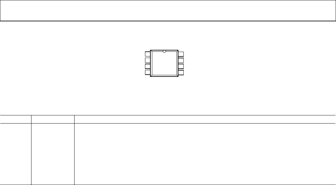
Figure 6. Pin Configuration
Table 4. Pin Function Descriptions
Pin No. Mnemonic Description
1 REF(−) Negative Reference Voltage Input.
2 −IN Inverting Input.
3 +IN Noninverting Input.
4 −V
S
Negative Supply Voltage.
5 REF(+) Positive Reference Voltage Input.
6 OUTPUT Output.
7 +V
S
Positive Supply Voltage.
8 NC No Connect. Do not connect to this pin.

AD629BR-REEL

Mfr. #:
Manufacturer:
Analog Devices Inc.
Description:
Differential Amplifiers High CM Vltg
Lifecycle:
New from this manufacturer.
Delivery:
DHL FedEx Ups TNT EMS
Payment:
T/T Paypal Visa MoneyGram Western Union