8Mb
SMART 3 BOOT BLOCK FLASH MEMORY
09005aef81136a91 Micron Technology, Inc., reserves the right to change products or specifications without notice.
Q10.fm - Rev. E 6/04 EN
19 ©2001 Micron Technology, Inc. All rights reserved.
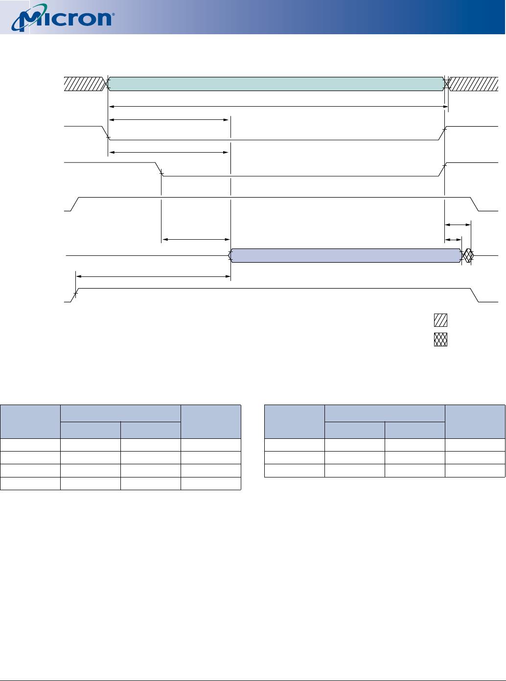
NOTE:
1. Vcc = MAX Vcc during ICC tests.
2. I
CC is dependent on cycle rates.
3. I
CC is dependent on output loading. Specified values are obtained with the outputs open.
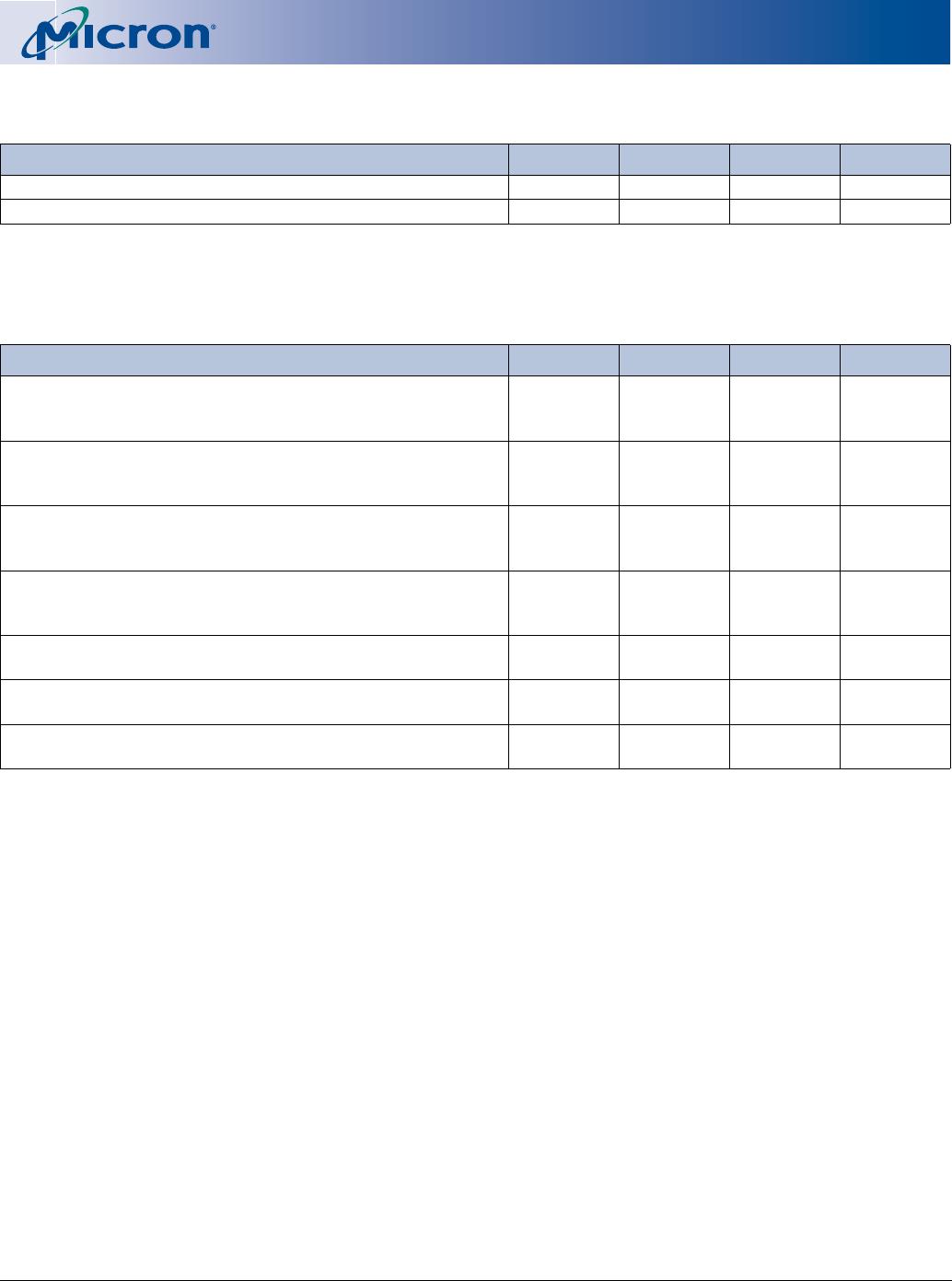
Table 10: Capacitance
(T
A
= 25°C; f = 1 MHz)
PARAMETER/CONDITION SYMBOL MAX UNITS NOTES
Input Capacitance
C
I 9pF
Output Capacitance
C
O 12 pF
Table 11: READ and STANDBY Current Drain
1
Commercial Temperature (0°C T
A
+70°C) and Extended Temperature (-40°C T
A
+85°C)
PARAMETER/CONDITION SYMBOL MAX UNITS NOTES
READ CURRENT: WORD-WIDE
(CE# 0.2V; OE# Vcc - 0.2V; f = 5 MHz;
Other inputs 0.2V or Vcc - 0.2V; RP# Vcc - 0.2V)
I
CC115mA2, 3
READ CURRENT: BYTE-WIDE
(CE# 0.2V; OE# Vcc - 0.2V; f = 5 MHz;
Other inputs 0.2V or Vcc - 0.2V; RP# = Vcc - 0.2V)
I
CC215mA2, 3
STANDBY CURRENT: TTL INPUT LEVELS
Vcc power supply standby current
(CE# = RP# = V
IH; Other inputs = VIL or VIH)
I
CC32mA
STANDBY CURRENT: CMOS INPUT LEVELS
Vcc power supply standby current
(CE# = RP# = Vcc - 0.2V)
I
CC4100 µA
DEEP POWER-DOWN CURRENT: Vcc SUPPLY
(RP# = V
SS ±0.2V)
ICC620 µA
STANDBY OR READ CURRENT: V
PP SUPPLY
(V
PP 5.5V)
I
PP15 µA
DEEP POWER-DOWN CURRENT: V
PP SUPPLY
(RP# = VSS ±0.2V)
I
PP25 µA
8Mb
SMART 3 BOOT BLOCK FLASH MEMORY
09005aef81136a91 Micron Technology, Inc., reserves the right to change products or specifications without notice.
Q10.fm - Rev. E 6/04 EN
20 ©2001 Micron Technology, Inc. All rights reserved.
NOTE:
1. Vcc = MAX Vcc during ICC tests. ICC is dependent on cycle rates.
2. ICC is dependent on output loading. Specified values are obtained with the outputs open.
AC Test Conditions
Input pulse levels. . . . . . . . . . . . . . . . . . . . . . . . . . 0V to 3V
Input rise and fall times . . . . . . . . . . . . . . . . . . . . . . .<10ns
Input timing reference level . . . . . . . . . . . . . . . . . . . . 1.5V
Output timing reference level. . . . . . . . . . . . . . . . . . . 1.5V
Output load. . . . . . . . . . . . . . . . 1TTL gate and CL = 50pF
Table 12: READ Timing Parameters Electrical Characteristics and Recommended
AC Operating Conditions
1
Commercial Temperature (0°C T
A
+70°C) and Extended Temperature (-40°C T
A
+85°C); Vcc = +3.3V ±0.3V
AC CHARACTERISTICS
SYMBOL
-9/-9 ET
UNITS NOTESPARAMETER MIN MAX
READ cycle time
t
RC
90 ns
Access time from CE#
t
ACE
90 ns 2
Access time from OE#
t
AOE
40 ns 2
Access time from address
t
AA
90 ns
RP# HIGH to output valid delay
t
RWH
1,000 ns
OE# or CE# HIGH to output in High-Z
t
OD
25 ns
Output hold time from OE#, CE# or address change
t
OH
0ns
RP# LOW pulse width
t
RP
150 ns
8Mb
SMART 3 BOOT BLOCK FLASH MEMORY
09005aef81136a91 Micron Technology, Inc., reserves the right to change products or specifications without notice.
Q10.fm - Rev. E 6/04 EN
21 ©2001 Micron Technology, Inc. All rights reserved.
Figure 10: Word-Wide READ Cycle
1
Timing Parameters
Commercial Temperature (0ºC T
A
+70ºC)
Extended Temperature (-40ºC T
A
+85ºC)
NOTE:
1. BYTE# = HIGH (MT28F800B3 only).
VALID DATA
VALID ADDRESS
CE#
A0–A18/(A19)
OE#
DQ0–DQ15
t
RC
t
ACE
t
AOE
t
OD
t
OH
t
AA
WE#
RP#
V
IH
V
IL
V
IH
V
IL
V
IH
V
IL
V
IH
V
IL
V
IH
V
IL
V
IH
VIL
t
RWH
DON’T CARE
UNDEFINED
SYMBOL
-9/-9 ET
UNITSMIN MAX
t
RC
90 ns
t
ACE
90 ns
t
AOE
40 ns
t
AA
90 ns
t
RWH
1,000 ns
t
OD
25 ns
t
OH
0ns
SYMBOL
-9/-9 ET
UNITSMIN MAX

MT28F800B3WG-9 B

Mfr. #:
Manufacturer:
Micron
Description:
IC FLASH 8M PARALLEL 48TSOP I
Lifecycle:
New from this manufacturer.
Delivery:
DHL FedEx Ups TNT EMS
Payment:
T/T Paypal Visa MoneyGram Western Union