8Mb
SMART 3 BOOT BLOCK FLASH MEMORY
09005aef81136a91 Micron Technology, Inc., reserves the right to change products or specifications without notice.
Q10.fm - Rev. E 6/04 EN
25 ©2001 Micron Technology, Inc. All rights reserved.
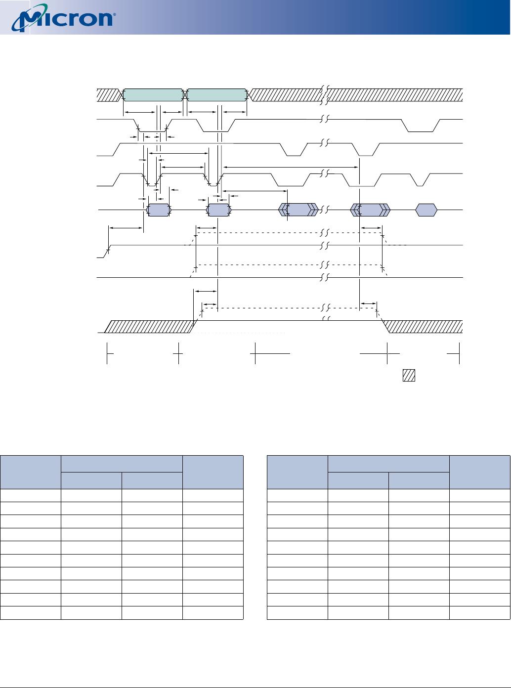
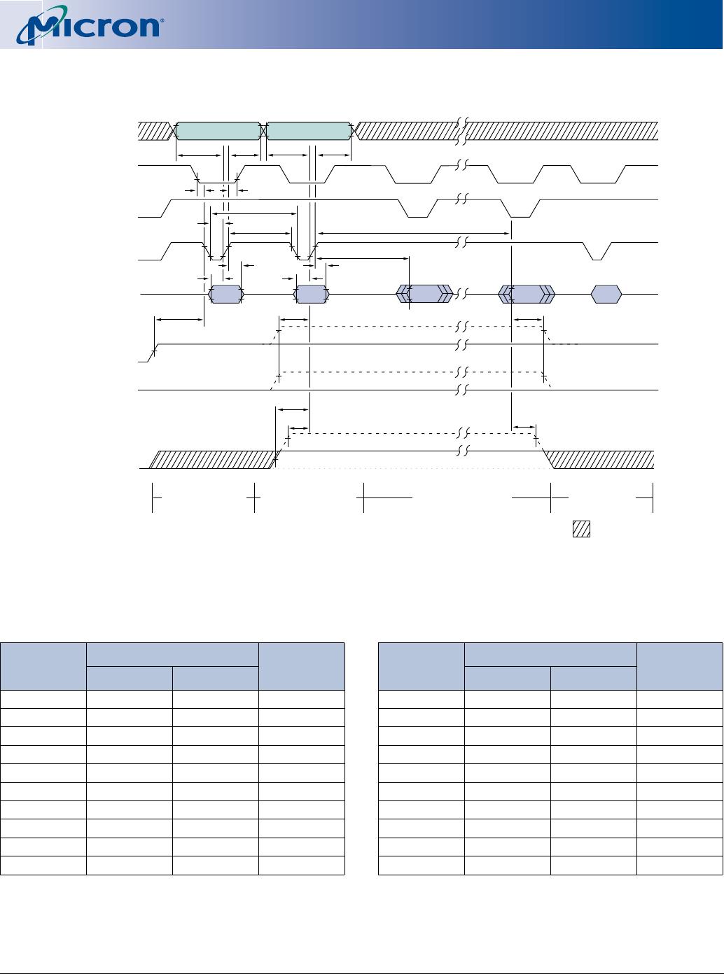
Figure 12: WRITE/ERASE Cycle
WE#-Controlled WRITE/ERASE
Timing Parameters
Commercial Temperature (0°C T
A
+70°C)
Extended Temperature (-40°C T
A
+85°C)
NOTE:
1. Address inputs are “Don’t Care” but must be held stable.
2. If BYTE# is LOW, data and command are 8-bit. If BYTE# is HIGH, data is 16-bit and command is 8-bit.
3. Either RP# at V
HH or WP# HIGH unlocks the boot block.
DON’T CARE
t
WC
t
WED1/2/3/4
t
RS
AIN
Status
(SR7=1)
t
CH
t
CS
[Unlock boot block]
t
RHS
t
AS
t
AH
t
WP
t
WPH
t
DS
t
DH
CMD
in
t
RHH
CMD/
Data-in
CMD
in
WRITE SETUP or
ERASE SETUP input
WRITE or ERASE (block)
address asserted, and
WRITE data or ERASE
CONFIRM issued
WRITE or ERASE
executed, status register
checked for completion
Command for next
operation issued
t
DH
t
DS
[Unlock boot block]
Note 1
t
AS
t
AH
Status
(SR7=0)
t
WB
CE#
A0–A18/(A19)
OE#
DQ0–DQ7/
DQ0–DQ15
2
WE#
RP#
3
V
IH
V
IL
VPP
V
IH
V
IL
V
HH
V
PPH1
V
PPH2
V
IH
V
IL
V
IH
V
IL
V
IH
V
IL
V
IH
V
IL
WP#
3
V
IH
V
IL
V
IL
t
VPS2
t
VPH
t
VPS1
[5V VPP]
[3.3V VPP]
SYMBOL
-9/-9 ET
UNITSMIN MAX
t
WC
90 ns
t
WPH
20 ns
t
WP
50 ns
t
AS
50 ns
t
AH
0ns
t
DS
50 ns
t
DH
0ns
t
CS
0ns
t
CH
0ns
t
VPS1
200 ns
t
VPS2
100 ns
t
RS
1,000 ns
t
RHS
100 ns
t
WED1
s
t
WED2
100 ms
t
WED3
100 ms
t
WED4
500 ms
t
WB
200 ns
t
VPH
0ns
t
RHH
0ns
SYMBOL
-9/-9 ET
UNITSMIN MAX
8Mb
SMART 3 BOOT BLOCK FLASH MEMORY
09005aef81136a91 Micron Technology, Inc., reserves the right to change products or specifications without notice.
Q10.fm - Rev. E 6/04 EN
26 ©2001 Micron Technology, Inc. All rights reserved.
Figure 13: WRITE/ERASE Cycle
CE#-Controlled WRITE/ERASE
Timing Parameters
Commercial Temperature (0°C T
A
+70°C)
Extended Temperature (-40°C T
A
+85°C)
NOTE:
1. Address inputs are “Don’t Care” but must be held stable.
2. If BYTE# is LOW, data and command are 8-bit. If BYTE# is HIGH, data is 16-bit and command is 8-bit.
3. Either RP# at V
HH or WP# HIGH unlocks the boot block.
DON’T CARE
t
WC
t
WED1/2/3/4
t
RS
AIN
Status
(SR7=1)
t
WH
t
WS
[Unlock boot block]
t
VPS2
t
RHS
t
VPH
t
AS
t
AH
t
CP
t
CPH
t
DS
t
DH
CMD
in
t
RHH
CMD/
Data-in
CMD
in
WRITE SETUP or
ERASE SETUP input
WRITE or ERASE (block)
address asserted, and
WRITE data or ERASE
CONFIRM issued
WRITE or ERASE
executed, status register
checked for completion
Command for next
operation issued
t
DH
t
DS
[Unlock boot block]
t
VPS1
Note 1
t
AS
t
AH
Status
(SR7=0)
t
WB
WE#
A0–A18/(A19)
OE#
DQ0–DQ7/
DQ0–DQ15
2
CE#
RP#
3
V
IH
V
IL
VPP
V
IH
V
IL
V
HH
V
PPH1
V
PPH2
V
IH
V
IL
V
IH
V
IL
V
IH
V
IL
V
IH
V
IL
WP#
3
V
IH
V
IL
V
IL
[5V VPP]
[3.3V VPP]
SYMBOL
-9/-9 ET
UNITSMIN MAX
t
WC
90 ns
t
CPH
20 ns
t
CP
50 ns
t
AS
50 ns
t
AH
0ns
t
DS
50 ns
t
DH
0ns
t
WS
0ns
t
WH
0ns
t
VPS1
200 ns
t
VPS2
100 ns
t
RS
1,000 ns
t
RHS
100 ns
t
WED1
s
t
WED2
100 ms
t
WED3
100 ms
t
WED4
500 ms
t
WB
200 ns
t
VPH
0ns
t
RHH
0ns
SYMBOL
-9/-9 ET
UNITSMIN MAX
8Mb
SMART 3 BOOT BLOCK FLASH MEMORY
09005aef81136a91 Micron Technology, Inc., reserves the right to change products or specifications without notice.
Q10.fm - Rev. E 6/04 EN
27 ©2001 Micron Technology, Inc. All rights reserved.
Figure 14: 40-Pin Plastic TSOP I
(10mm x 20mm)
NOTE:
1. All dimensions in millimeters.
2. Package width and length do not include mold protrusion; allowable mold protrusion is .01” per side.
DETAIL A
0.50 TYP
SEE DETAIL A
0.10
0.80
0.5 ±0.1
1.20 MAX
0.25
GAGE
PLANE
0.25
FOR REFERENCE
ONLY
10.00 ±0.08
20.00 ±0.10
18.40 ±0.08
PIN #1 INDEX
0.15
+0.03
-0.02
0.10
+0.10
-0.05
0.20 ±0.05
PLATED LEAD FINISH: 90% Sn, 10% Pb, OR 100% Sn
PLASTIC PACKAGE MATERIAL: NOVOLAC EPOXY
PACKAGE WIDTH AND LENGTH DO NOT
INCLUDE MOLD PROTRUSION. ALLOWABLE
PROTRUSION IS 0.25 PER SIDE.

MT28F800B3WG-9 B

Mfr. #:
Manufacturer:
Micron
Description:
IC FLASH 8M PARALLEL 48TSOP I
Lifecycle:
New from this manufacturer.
Delivery:
DHL FedEx Ups TNT EMS
Payment:
T/T Paypal Visa MoneyGram Western Union