LTC2605/LTC2615/LTC2625
10
2605fa
PIN FUNCTIONS
BLOCK DIAGRAM
TIMING DIAGRAM
GND (Pin 1): Analog Ground.
V
OUT A
to V
OUT H
(Pins 2-5 and 12-15): DAC Analog Volt-
age Output. The output range is 0V to V
REF
.
REF (Pin 6): Reference Voltage Input. 0V ≤ V
REF
≤ V
CC
.
CA2 (Pin 7): Chip Address Bit 2. Tie this pin to V
CC
, GND
or leave it fl oating to select an I
2
C slave address for the
part (Table 2).
SCL (Pin 8): Serial Clock Input Pin. Data is shifted into
the SDA pin at the rising edges of the clock. This high
impedance pin requires a pull-up resistor or current
source to V
CC
.
SDA (Pin 9): Serial Data Bidirectional Pin. Data is shifted
into the SDA pin and acknowledged by the SDA pin. This
is a high impedance pin while data is shifted in. It is an
open-drain N-channel output during acknowledgment. This
pin requires a pull-up resistor or current source to V
CC
.
CA1 (Pin 10): Chip Address Bit 1. Tie this pin to V
CC
, GND
or leave it fl oating to select an I
2
C slave address for the
part (Table 2).
CA0 (Pin 11): Chip Address Bit 0. Tie this pin to V
CC
, GND
or leave it fl oating to select an I
2
C slave address for the
part (Table 2).
V
CC
(Pin 16): Supply Voltage Input. 2.7V ≤ V
CC
≤ 5.5V.
2
15
1GND
V
OUT A
V
OUT B
V
OUT C
V
OUT D
REF
CA2
SCL
V
CC
V
OUT H
V
OUT G
V
OUT F
V
OUT E
CA0
CA1
SDA
2605 BD01
16
DAC A
3 14
4 13
5
7
6
8
10
11
9
12
2-WIRE INTERFACE
32-BIT SHIFT REGISTER
DAC
REGISTER
DAC
REGISTER
DAC
REGISTER
DAC
REGISTER
DAC
REGISTER
DAC
REGISTER
DAC
REGISTER
DAC
REGISTER
INPUT
REGISTER
INPUT
REGISTER
INPUT
REGISTER
INPUT
REGISTER
INPUT
REGISTER
INPUT
REGISTER
INPUT
REGISTER
INPUT
REGISTER
DAC H
DAC B DAC G
DAC C DAC F
DAC D DAC E
SDA
t
f
S
t
r
t
LOW
t
HD(STA)
ALL VOLTAGE LEVELS REFER TO V
IH(MIN)
AND V
IL(MAX)
LEVELS
t
HD(DAT)
t
SU(DAT)
t
SU(STA)
t
HD(STA)
t
SU(STO)
t
SP
t
BUF
t
r
t
f
t
HIGH
SCL
S P S
2605 F01
Figure 1
LTC2605/LTC2615/LTC2625
11
2605fa
OPERATION
Power-On Reset
The LTC2605/LTC2615/LTC2625 clear the outputs to
zero-scale when power is fi rst applied, making system
initialization consistent and repeatable. The LTC2605-1/
LTC2615-1/LTC2625-1 set the voltage outputs to mid-scale
when power is fi rst applied.
For some applications, downstream circuits are active dur-
ing DAC power-up, and may be sensitive to nonzero outputs
from the DAC during this time. The LTC2605/LTC2615/
LTC2625 contain circuitry to reduce the power-on glitch:
the analog outputs typically rise less than 10mV above
zero-scale during power on if the power supply is ramped
to 5V in 1ms or more. In general, the glitch amplitude
decreases as the power supply ramp time is increased.
See Power-On Reset Glitch in the Typical Performance
Characteristics section.
Power Supply Sequencing
The voltage at REF (Pin 6) should be kept within the range
–0.3V ≤ V
REF
≤ V
CC
+ 0.3V (see Absolute Maximum Rat-
ings). Particular care should be taken to observe these
limits during power supply turn-on and turn-off sequences,
when the voltage at V
CC
(Pin 16) is in transition.
Transfer Function
The digital-to-analog transfer function is:
V
k
V
OUT IDEAL
N
REF()
=
2
where k is the decimal equivalent of the binary DAC input
code, N is the resolution and V
REF
is the voltage at REF
(Pin 6).
Serial Digital Interface
The LTC2605/LTC2615/LTC2625 communicate with a
host using the standard 2-wire digital interface. The Tim-
ing Diagram (Figure 1) shows the timing relationship of
the signals on the bus. The two bus lines, SDA and SCL,
must be high when the bus is not in use. External pull-up
resistors or current sources are required on these lines.
The value of these pull-up resistors is dependent on the
power supply and can be obtained from the I
2
C specifi ca-
tions. For an I
2
C bus operating in the fast mode, an active
pull-up will be necessary if the bus capacitance is greater
than 200pF. The V
CC
power should not be removed from
the LTC2605/LTC2615/LTC2625 when the I
2
C bus is active
to avoid loading the I
2
C bus lines through the internal ESD
protection diodes.
The LTC2605/LTC2615/LTC2625 are receive-only (slave)
devices. The master can write to the LTC2605/LTC2615/
LTC2625. The LTC2605/LTC2615/LTC2625 do not respond
to a read from the master.
The START (S) and STOP (P) Conditions
When the bus is not in use, both SCL and SDA must be
high. A bus master signals the beginning of a communica-
tion to a slave device by transmitting a START condition. A
START condition is generated by transitioning SDA from
high to low while SCL is high.
Table 1
COMMAND*
C3 C2 C1 C0
0 0 0 0 Write to Input Register n
0 0 0 1 Update (Power Up) DAC Register n
0 0 1 0 Write to Input Register n, Update (Power Up) All n
0 0 1 1 Write to and Update (Power Up) n
0 1 0 0 Power Down n
1 1 1 1 No Operation
*Address and command codes not shown are reserved and should not
be used.
ADDRESS (n)*
A3 A2 A1 A0
0 0 0 0 DAC A
0 0 0 1 DAC B
0 0 1 0 DAC C
0 0 1 1 DAC D
0 1 0 0 DAC E
0 1 0 1 DAC F
0 1 1 0 DAC G
0 1 1 1 DAC H
1 1 1 1 All DACs
LTC2605/LTC2615/LTC2625
12
2605fa
OPERATION
When the master has fi nished communicating with the
slave, it issues a STOP condition. A STOP condition is
generated by transitioning SDA from low to high while
SCL is high. The bus is then free for communication with
another I
2
C device.
Acknowledge
The Acknowledge signal is used for handshaking between
the master and the slave. An Acknowledge (active LOW)
generated by the slave lets the master know that the lat-
est byte of information was received. The Acknowledge
related clock pulse is generated by the master. The master
releases the SDA line (HIGH) during the Acknowledge
clock pulse. The slave-receiver must pull down the SDA
during the Acknowledge clock pulse so that it remains a
stable LOW during the HIGH period of this clock pulse.
The LTC2605/LTC2615/LTC2625 respond to a write by a
master in this manner. The LTC2605/LTC2615/LTC2625 do
not acknowledge a read (it retains SDA HIGH during the
period of the Acknowledge clock pulse).
Chip Address
The state of CA0, CA1 and CA2 decides the slave address
of the part. The pins CA0, CA1 and CA2 can be each set to
any one of three states: V
CC
, GND or FLOAT. This results
in 27 selectable addresses for the part. The addresses
corresponding to the states of CA0, CA1 and CA2 and the
global address are shown in Table 2.
In addition to the address selected by the address pins,
the parts also respond to a global address. This address
allows a common write to all LTC2605, LTC2615 and
LTC2625 parts to be accomplished with one 3-byte write
transaction on the I
2
C bus. The global address is a 7-bit
hard-wired address and is not selectable by CA0, CA1 and
CA2. The maximum capacitive load allowed on the address
pins (CA0, CA1 and CA2) is 10pF.
Write Word Protocol
The master initiates communication with the LTC2605/
LTC2615/LTC2625 with a START condition and a 7-bit slave
address followed by the Write bit (W) = 0. The LTC2605/
LTC2615/LTC2625 acknowledges by pulling the SDA pin
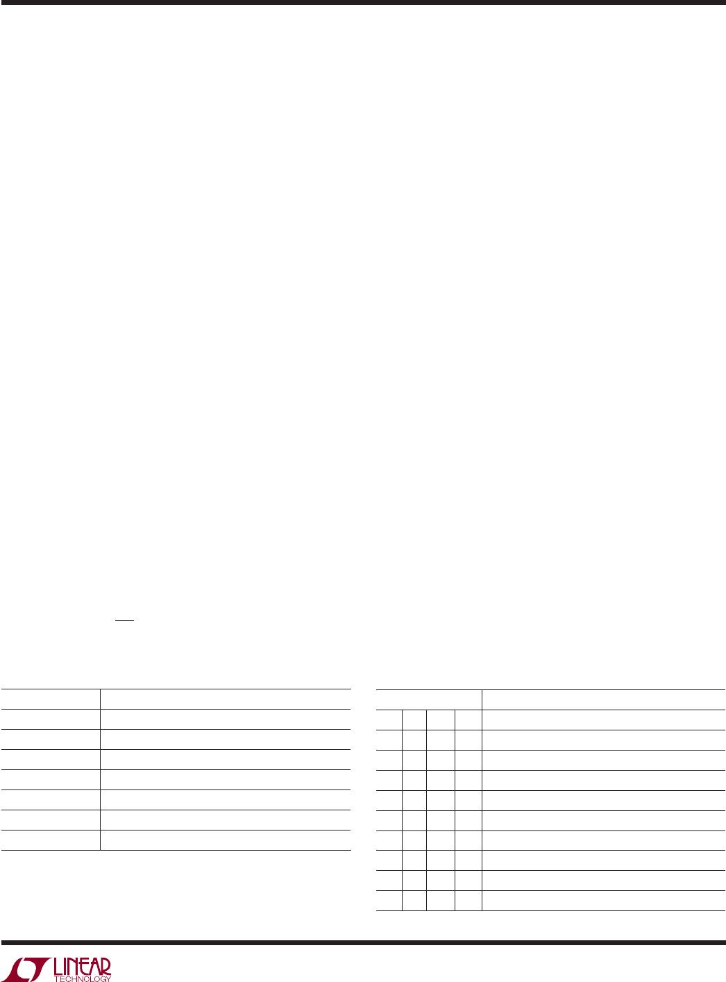
Table 2. Slave Address Map
CA2 CA1 CA0 SA6 SA5 SA4 SA3 SA2 SA1 SA0
GND GND GND 0 0 1 0 0 0 0
GNDGNDFLOAT0010001
GND GND V
CC
0010010
GNDFLOATGND0010011
GNDFLOATFLOAT0100000
GNDFLOATVCC0100001
GND V
CC
GND0100010
GND V
CC
FLOAT0100011
GND V
CC
V
CC
0110000
FLOATGNDGND0110001
FLOATGNDFLOAT0110010
FLOAT GND V
CC
0110011
FLOATFLOATGND1000000
FLOAT FLOAT FLOAT 1 0 0 0 0 0 1
FLOAT FLOAT V
CC
1000010
FLOAT V
CC
GND1000011
FLOAT V
CC
FLOAT1010000
FLOAT V
CC
V
CC
1010001
V
CC
GNDGND1010010
V
CC
GNDFLOAT1010011
V
CC
GND V
CC
1100000
V
CC
FLOATGND1100001
V
CC
FLOATFLOAT1100010
V
CC
FLOAT V
CC
1100011
V
CC
V
CC
GND1110000
V
CC
V
CC
FLOAT1110001
V
CC
V
CC
V
CC
1110010
GLOBAL ADDRESS 1 1 1 0 0 1 1
low at the 9th clock if the 7-bit slave address matches the
address of the parts (set by CA0, CA1 and CA2) or the
global address. The master then transmits three bytes of
data. The LTC2605/LTC2615/LTC2625 acknowledges each
byte of data by pulling the SDA line low at the 9th clock of
each data byte transmission. After receiving three complete
bytes of data, the LTC2605/LTC2615/LTC2625 executes the
command specifi ed in the 24-bit input word.
If more than three data bytes are transmitted after a valid
7-bit slave address, the LTC2605/LTC2615/LTC2625 do not
acknowledge the extra bytes of data (SDA is high during
the 9th clock).

LTC2605CGN#PBF

Mfr. #:
Manufacturer:
Analog Devices Inc.
Description:
Digital to Analog Converters - DAC Octal I2C 16-B R2R DACs in 16-Lead SSOP
Lifecycle:
New from this manufacturer.
Delivery:
DHL FedEx Ups TNT EMS
Payment:
T/T Paypal Visa MoneyGram Western Union