LTC2605/LTC2615/LTC2625
4
2605fa
ELECTRICAL CHARACTERISTICS
The l denotes the specifi cations which apply over the full operating
temperature range, otherwise specifi cations are at T
A
= 25°C. REF = 4.096V (V
CC
= 5V), REF = 2.048V (V
CC
= 2.7V), V
OUT
unloaded,
unless otherwise noted. (Note 9)
SYMBOL PARAMETER CONDITIONS MIN TYP MAX UNITS
Digital I/O (Note 9)
V
IL
Low Level Input Voltage (SDA and SCL)
l
0.3V
CC
V
V
IH
High Level Input Voltage (SDA and SCL)
l
0.7V
CC
V
V
IL(CA)
Low Level Input Voltage (CA0 to CA2) See Test Circuit 1
l
0.15V
CC
V
V
IH(CA)
High Level Input Voltage (CA0 to CA2) See Test Circuit 1
l
0.85V
CC
V
R
INH
Resistance from CAn (n = 0,1,2) to V
CC
to Set CAn = V
CC
See Test Circuit 2
l
10
R
INL
Resistance from CAn (n = 0,1,2) to GND
to Set CAn = GND
See Test Circuit 2
l
10
R
INF
Resistance from CAn (n = 0,1,2) to V
CC
or GND to Set CAn = FLOAT
See Test Circuit 2
l
2MΩ
V
OL
Low Level Output Voltage Sink Current = 3mA
l
0 0.4 V
t
OF
Output Fall Time V
O
= V
IH(MIN)
to V
O
= V
IL(MAX)
, C
B
= 10pF to 400pF
(Note 7)
l
20 + 0.1CB 250 ns
t
SP
Pulse Width of Spikes Surpassed by
Input Filter
l
050ns
I
IN
Input Leakage 0.1V
CC
≤ V
IN
≤ 0.9V
CC
l
A
C
IN
I/O Pin Capacitance (Note 12)
l
10 pF
C
B
Capacitance Load for Each Bus Line
l
400 pF
C
CAn
External Capacitive Load on Address
Pins CA0, CA1 and CA2
l
10 pF
The l denotes the specifi cations which apply over the full operating temperature range, otherwise specifi cations are at T
A
= 25°C.
REF = 4.096V (V
CC
= 5V), REF = 2.048V (V
CC
= 2.7V), V
OUT
unloaded, unless otherwise noted.
SYMBOL PARAMETER CONDITIONS
LTC2625/LTC2625-1 LTC2615/LTC2615-1 LTC2605/LTC2605-1
UNITSMIN TYP MAX MIN TYP MAX MIN TYP MAX
AC Performance
t
S
Settling Time (Note 5) ±0.024% (±1LSB at 12 Bits)
±0.006% (±1LSB at 14 Bits)
±0.0015% (±1LSB at 16 Bits)
77
9
7
9
10
μs
μs
μs
Settling Time for 1LSB Step
(Note 6)
±0.024% (±1LSB at 12 Bits)
±0.006% (±1LSB at 14 Bits)
±0.0015% (±1LSB at 16 Bits)
2.7 2.7
4.8
2.7
4.8
5.2
μs
μs
μs
Voltage Output Slew Rate 0.80 0.80 0.80 V/μs
Capacitive Load Driving 1000 1000 1000 pF
Glitch Inpulse At Mid-Scale Transition 12 12 12 nV•s
Multiplying Bandwidth 180 180 180 kHz
e
n
Output Voltage Noise Density At f = 1kHz
At f = 10kHz
120
100
120
100
120
100
nV/√Hz
nV/√Hz
Output Voltage Noise 0.1Hz to 10Hz 15 15 15 μV
P-P
LTC2605/LTC2615/LTC2625
5
2605fa
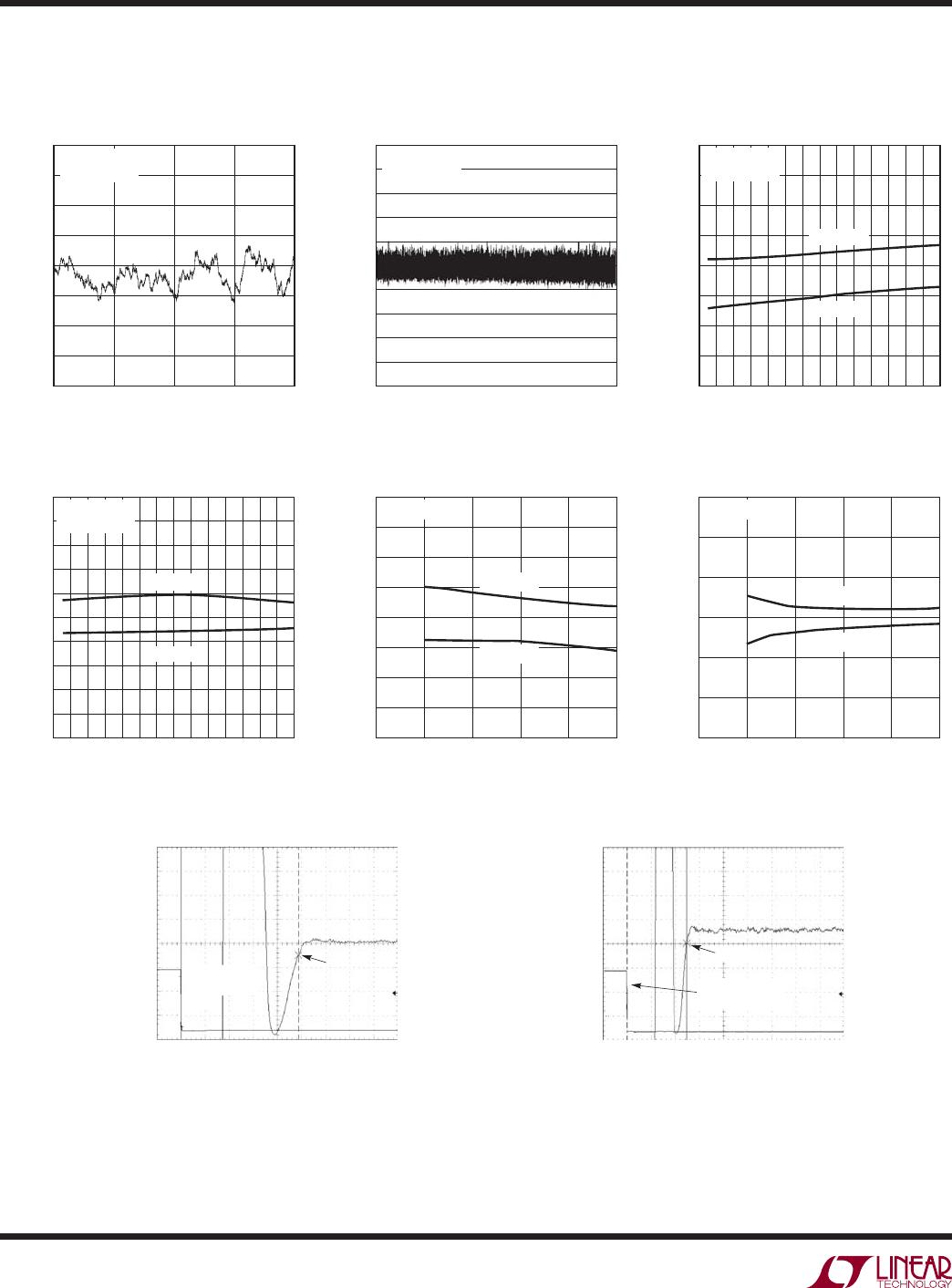
TIMING CHARACTERISTICS
The l denotes the specifi cations which apply over the full operating temperature
range, otherwise specifi cations are at T
A
= 25°C. See Figure 1. (Notes 8, 9)
SYMBOL PARAMETER CONDITIONS MIN TYP MAX UNITS
V
CC
= 2.7V to 5.5V
f
SCL
SCL Clock Frequency
l
0 400 kHz
t
HD(STA)
Hold Time (Repeated) Start Condition
l
0.6 μs
t
LOW
Low Period of the SCL Clock Pin
l
1.3 μs
t
HIGH
High Period of the SCL Clock Pin
l
0.6 μs
t
SU(STA)
Set-Up Time for a Repeated Start Program
l
0.6 μs
t
HD(DAT)
Data Hold Time
l
0 0.9 μs
t
SU(DAT)
Data Set-Up Time
l
100 ns
t
r
Rise Time of Both SDA and SCL Signals (Note 7)
l
20 + 0.1CB 300 ns
t
f
Fall Time of Both SDA and SCL Signals (Note 7)
l
20 + 0.1CB 300 ns
t
SU(STO)
Set-Up Time for Stop Condition
l
0.6 μs
t
BUF
Bus Free Time Between a Stop and Start Condition
l
1.3 μs
Note 1: Stresses beyond those listed under Absolute Maximum Ratings
may cause permanent damage to the device. Exposure to any Absolute
Maximum Rating condition for extended periods may affect device
reliability and lifetime.
Note 2: Linearity and monotonicity are defi ned from code k
L
to code
2
N
– 1, where N is the resolution and k
L
is given by k
L
= 0.016(2
N
/V
REF
),
rounded to the nearest whole code. For V
REF
= 4.096V and N = 16,
k
L
= 256 and linearity is defi ned from code 256 to code 65,535.
Note 3: SDA, SCL at 0V or V
CC
, CA0, CA1 and CA2 fl oating.
Note 4: Inferred from measurement at code 256 (LTC2605/LTC2605-1),
code 64 (LTC2615/LTC2615-1) or code 16 (LTC2625/LTC2625-1) and at
full-scale.
Note 5: V
CC
= 5V, V
REF
= 4.096V. DAC is stepped 1/4-scale to 3/4-scale and
3/4-scale to 1/4-scale. Load is 2kΩ in parallel with 200pF to GND.
Note 6: V
CC
= 5V, V
REF
= 4.096V. DAC is stepped ±1LSB between half-scale
and half-scale – 1. Load is 2kΩ in parallel with 200pF to GND.
Note 7: C
B
= capacitance of one bus line in pF.
Note 8: All values refer to V
IH(MIN)
and V
IL(MAX)
levels.
Note 9: These specifi cations apply to LTC2605/LTC2605-1,
LTC2615/LTC2615-1 and LTC2625/LTC2625-1.
Note 10: DC Crosstalk is measured with V
CC
= 5V and V
REF
= 4096V, with
the measured DAC at mid-scale, unless otherwise noted.
Note 11: R
L
= 2kΩ to GND or V
CC
.
Note 12: Guaranteed by design and not production tested.
ELECTRICAL CHARACTERISTICS
Test Circuit 1 Test Circuit 2
V
IH(CA
n
)
/V
IL(CA
n
)
CAn
100Ω
2605 TC01
GND
R
INH
/R
INL
/R
INF
V
DD
2605 TC02
LTC2605/LTC2615/LTC2625
6
2605fa
TYPICAL PERFORMANCE CHARACTERISTICS
DNL vs Temperature INL vs V
REF
DNL vs V
REF
Settling to ±1LSB Settling of Full-Scale Step
Integral Nonlinearity (INL) Differential Nonlinearity (DNL) INL vs Temperature
LTC2605
CODE
0
16384 32768 49152 65535
INL (LSB)
2605 G01
32
24
16
8
0
–8
–16
–24
–32
V
CC
= 5V
V
REF
= 4.096V
CODE
0 16384 32768 49152 65535
DNL (LSB)
2605 G02
1.0
0.8
0.6
0.4
0.2
0
–0.2
–0.4
–0.6
–0.8
–1.0
V
CC
= 5V
V
REF
= 4.096V
TEMPERATURE (°C)
–50
–30 –10 10 30 50 70 90
INL (LSB)
2605 G03
32
24
16
8
0
–8
–16
–24
–32
V
CC
= 5V
V
REF
= 4.096V
INL (POS)
INL (NEG)
TEMPERATURE (°C)
–50
–30 –10 10 30 50 70 90
DNL (LSB)
2605 G04
1.0
0.8
0.6
0.4
0.2
0
–0.2
–0.4
–0.6
–0.8
–1.0
V
CC
= 5V
V
REF
= 4.096V
DNL (POS)
DNL (NEG)
V
REF
(V)
0
1 2 3 4 5
INL (LSB)
2605 G05
32
24
16
8
0
–8
–16
–24
–32
V
CC
= 5.5V
INL (POS)
INL (NEG)
V
REF
(V)
0
1 2 3 4 5
DNL (LSB)
2605 G06
1.5
1.0
0.5
0
–0.5
–1.0
–1.5
V
CC
= 5.5V
DNL (POS)
DNL (NEG)
2μs/DIV
2605 G07
V
OUT
100μV/DIV
SCL
2V/DIV
V
CC
= 5V, V
REF
= 4.096V
1/4-SCALE TO 3/4-SCALE STEP
R
L
= 2k, C
L
= 200pF
AVERAGE OF 2048 EVENTS
9.7μs
9TH CLOCK
OF 3RD DATA
BYTE
5μs/DIV
2605 G08
V
OUT
100μV/DIV
SCR
2V/DIV
SETTLING TO ±1LSB
V
CC
= 5V, V
REF
= 4.096V
CODE 512 TO 65535 STEP
AVERAGE OF 2048 EVENTS
12.3μs
9TH CLOCK OF
3RD DATA BYTE

LTC2605CGN#PBF

Mfr. #:
Manufacturer:
Analog Devices Inc.
Description:
Digital to Analog Converters - DAC Octal I2C 16-B R2R DACs in 16-Lead SSOP
Lifecycle:
New from this manufacturer.
Delivery:
DHL FedEx Ups TNT EMS
Payment:
T/T Paypal Visa MoneyGram Western Union