LTC1392CN8#PBF

4
LTC1392
RECOM ENDED OPERATING CONDITIONS
UUU
U
WW
The denotes specifications which apply over the operating temperature
range (0°C T
A
70°C for commercial grade and –40°C T
A
85°C for
industrial grade).
Note 1: Absolute maximum ratings are those values beyond which the life
of the device may be impaired.
Note 2: All voltage values are with respect to GND.
Note 3: Testing done at V
CC
= 5V, CLK = 250kHz and T
A
= 25°C unless
otherwise specified.
Note 4: Temperature integral nonlinearity is defined as the deviation of the
A/D code versus temperature curve from the best-fit straight line over the
device’s rated temperature range.
Note 5: Voltage integral nonlinearity is defined as the deviation of a code
from a straight line passing through the actual end points of the transfer
curve.
Note 6: Channel leakage current is measured after the channel selection.
Note 7: See guaranteed temperature limit curves vs temperature range on
the first page of this data sheet.
TYPICAL PERFORMANCE CHARACTERISTICS
U
W
Differential Nonlinearity
Power Supply Voltage Mode
Differential Nonlinearity
Integral Nonlinearity
Power Supply Voltage Mode
CODE
256
1.0
DIFFERENTIAL NONLINEARITY ERROR (LSB)
0.5
0
0.5
1.0
320 384 448 512
1392 G01
576 640 704 768 832
f
CLK
= 250kHz
T
A
= 25°C
CODE
256
1.0
INTEGRAL NONLINEARITY ERROR (LSB)
0.5
0
0.5
1.0
320 384 448 512
1392 G02
576 640 704 768 832
f
CLK
= 250kHz
T
A
= 25°C
CODE
2561280
1.0
DIFFERENTIAL NONLINEARITY ERROR (LSB)
0.5
0
0.5
1.0
384 512
1392 G03
640 768 896 1024
Full Scale = 1V
f
CLK
= 250kHz
T
A
= 25°C
V
CC
= 5V
CODE
2561280
1.0
INTEGRAL NONLINEARITY ERROR (LSB)
0.5
0
0.5
1.0
384 512
1392 G04
640 768 896 1024
Full Scale = 1V
f
CLK
= 250kHz
T
A
= 25°C
V
CC
= 5V
Integral Nonlinearity
Integral NonlinearityDifferential Nonlinearity
CODE
2561280
1.0
DIFFERENTIAL NONLINEARITY ERROR (LSB)
0.5
0
0.5
1.0
384 512
1392 G05
640 768 896 1024
Full Scale = 0.5V
f
CLK
= 250kHz
T
A
= 25°C
V
CC
= 5V
CODE
2561280
1.0
INTEGRAL NONLINEARITY ERROR (LSB)
0.5
0
0.5
1.0
384 512
1392 G06
640 768 896 1024
Full Scale = 0.5V
f
CLK
= 250kHz
T
A
= 25°C
V
CC
= 5V
5
LTC1392
TYPICAL PERFORMANCE CHARACTERISTICS
U
W
INPUT
SHIFT
REGISTER
BANDGAP
CONTROL
AND TIMING
CS
4
LTC1392 • BD
SERIAL
PORT
V
REF
= 2.42V
V
REF
= 1V
V
REF
= 0.5V
ANALOG
INPUT
MUX
10-BIT
SAR
10
BITS
C
SAMPLE
V
CC
85
GND
TEMPERATURE
SENSOR
V
CC
GND
D
IN
1
V
REF
+V
IN
–V
IN
6
7
COMP
10-BIT
CAPACITIVE DAC
+
+
+
D
OUT
2
CLK
3
BLOCK DIAGRAM
W
PIN FUNCTIONS
UUU
D
IN
(Pin 1): Digital Input. The A/D configuration word is
shifted into this input.
D
OUT
(Pin 2): Digital Output. The A/D result is shifted out
of this output.
CLK (Pin 3): Shift Clock. This clock synchronizes the serial
data.
CS (Pin 4): Chip Select Input. A logic low on this input
enables the LTC1392.
GND (Pin 5): Ground Pin. GND should be tied directly to
an analog ground plane.
+V
IN
(Pin 6): Positive Analog Differential Input. The pin
can be used as a single-ended input by grounding –V
IN
.
–V
IN
(Pin 7): Negative Analog Differential Input. The input
must be free from noise.
V
CC
(Pin8): Positive Supply. This supply must be kept free
from noise and ripple by bypassing directly to the ground
plane.
Supply Current vs Sample Rate
TIME (SEC)
0
TEMPERATURE (°C)
5
10
15 20
1392 G07
25
70
65
60
55
50
45
40
35
30
25
20
30
V
CC
= 5V
N8
S8
Thermal Response in Stirred
Oil Bath
SAMPLE FREQUENCY (Hz)
SUPPLY CURRENT (µA)
1000
100
10
1
0.1
0.1 10 100 1k 10k 100k
1392 G09
1
V
CC
= 5V
f
CLK
= 250kHz
T
A
= 25°C
CS LOW BETWEEN SAMPLES
CS HIGH BETWEEN
SAMPLES
TIME (SEC)
0
TEMPERATURE (°C)
50
100
150 200
1392 G08
250
70
65
60
55
50
45
40
35
30
25
20
300
V
CC
= 5V
N8
S8
Thermal Response in Still Air
6
LTC1392
TEST CIRCUITS
Voltage Waveforms for t
dis
D
OUT
WAVEFORM 1
(SEE NOTE 1)
2.0V
t
dis
90%
10%
D
OUT
WAVEFORM 2
(SEE NOTE 2)
CS
NOTE 1: WAVEFORM 1 IS FOR AN OUTPUT WITH INTERNAL CONDITIONS SUCH
THAT THE OUTPUT IS HIGH UNTIL DISABLED BY THE OUTPUT CONTROL.
NOTE 2: WAVEFORM 2 IS FOR AN OUTPUT WITH INTERNAL CONDITIONS SUCH
THAT THE OUTPUT IS LOW UNTIL DISABLED BY THE OUTPUT CONTROL.
LTC1392 • TC06
APPLICATIONS INFORMATION
WUU
U
DIGITAL CONSIDERATIONS
Serial Interface
The LTC1392 communicates with microprocessors and
other external circuitry via a synchronous, half-duplex,
3-wire serial interface (see Figure 1). The clock (CLK)
synchronizes the data transfer with each bit being trans-
mitted on the falling CLK edge and captured on the rising
CLK edge in both transmitting and receiving systems. The
input data is first received and then the A/D conversion
result is transmitted (half-duplex). Half-duplex operation
allows D
IN
and D
OUT
to be tied together allowing transmis-
sion over three wires: CS, CLK and DATA (D
IN
/D
OUT
). Data
transfer is initiated by a falling chip select (CS) signal. After
the falling CS is recognized, an 80µs delay is needed for
The LTC1392 is a micropower data acquisition system
designed to measure temperature, an on-chip power
supply voltage and a differential input voltage. The LTC1392
contains the following functional blocks:
1. On-chip temperature sensor
2. 10-bit successive approximation capacitive ADC
3. Bandgap reference
4. Analog multiplexer (MUX)
5. Sample-and-hold (S/H)
6. Synchronous, half-duplex serial interface
7. Control and timing logic
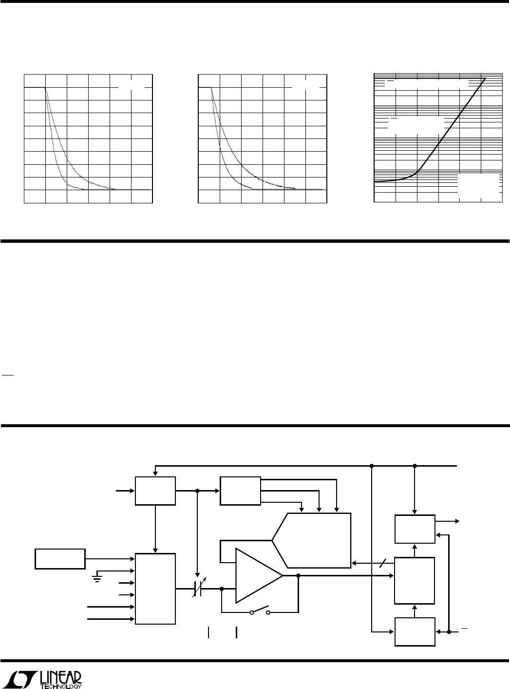
Load Circuit for t
dDO
, t
r
and t
f
D
OUT
1.4V
3k
100pF
TEST POINT
LTC1392 • TC02
Voltage Waveforms for D
OUT
Delay Time, t
dDO
CLK
D
OUT
V
IL
t
dDO
V
OL
V
OH
LTC1392 • TC03
Load Circuit for t
dis
and t
en
D
OUT
3k
100pF
TEST POINT
5V t
dis
WAVEFORM 2, t
en
t
dis
WAVEFORM 1
LTC1392 • TC05
Voltage Waveforms for D
OUT
Rise and Fall Times, t
r
and t
f
D
OUT
V
OL
V
OH
t
r
t
f
1392 TC04

LTC1392CN8#PBF

Mfr. #:
Manufacturer:
Analog Devices Inc.
Description:
Current & Power Monitors & Regulators Power Data Acquisition System
Lifecycle:
New from this manufacturer.
Delivery:
DHL FedEx Ups TNT EMS
Payment:
T/T Paypal Visa MoneyGram Western Union