LTC1392CN8#PBF

7
LTC1392
APPLICATIONS INFORMATION
WUU
U
MSB-First Data (MSBF = 1)
t
CYC
CS
START
SEL1 SEL0
SEL1 SEL0
MSBF
t
SMPL
Hi-Z Hi-Z
FILLED WITH ZEROS
D
IN
D
OUT
B9 B8 B7 B6 B5 B4 B3 B2 B1
t
CONV
B0
CLK
t
suCS
t
WAKEUP
t
CYC
CS
START MSBF
Hi-Z Hi-Z
LTC1392 • F01
FILLED WITH ZEROS
D
IN
D
OUT
B9 B8 B7 B6 B5 B4 B3 B2 B1
t
CONV
B0 B1 B2 B3 B4 B5 B6 B7 B8 B9
CLK
t
suCS
t
WAKEUP
t
SMPL
Figure 1
temperature measurement or a 10µs delay for other mea-
surements, followed by a 4-bit input word which config-
ures the LTC1392 for the current conversion. This data
word is shifted into the D
IN
input. D
IN
is then disabled from
shifting in any data and the D
OUT
pin is configured from
three-state to an output pin. A null bit and the result of the
current conversion are serially transmitted on the falling
CLK edge onto the D
OUT
line. The format of the A/D result
can be either MSB-first sequence or MSB-first sequence
followed by an LSB-first sequence. This provides easy
interface to MSB- or LSB-first serial ports. Bringing CS
high resets the LTC1392 for the next data exchange.
INPUT DATA WORD
Data transfer is initiated by a falling chip select (CS) signal.
After CS falls, the LTC1392 looks for a start bit. Once the
start bit is received, the next three bits are shifted into the
D
IN
input which configures the LTC1392 and starts the
conversion. Further inputs on the D
IN
input are then
ignored until the next CS cycle. The four bits of the input
word are defined as follows:
BIT 3 BIT 2 BIT 1 BIT 0
Start Select 1 Select 0 MSBF
Start Bit
The first “logic one” clocked into the D
IN
input after CS
goes low is the Start Bit. The Start Bit initiates the data
transfer and all leading zeros which precede this logical
one will be ignored. After the Start Bit is received the
remaining bits of the input word will be clocked in. Further
input on the D
IN
pin are then ignored until the next CS
cycle.
8
LTC1392
APPLICATIONS INFORMATION
WUU
U
Measurement Mode Selections
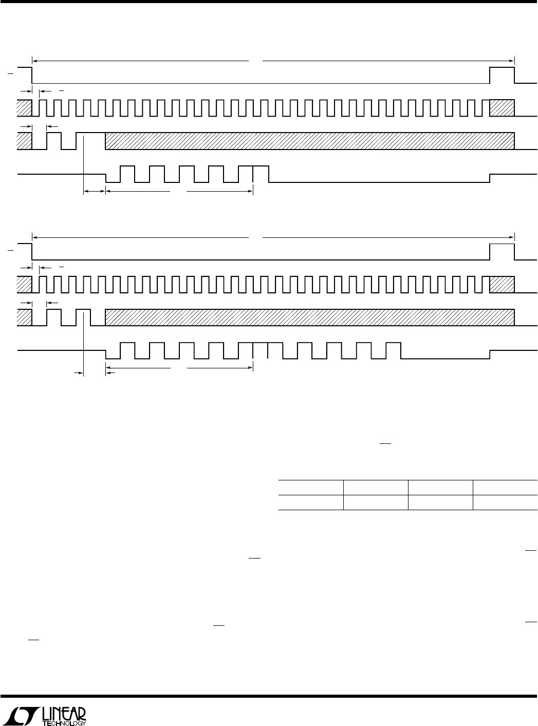
The two bits of the input word following the Start Bit assign
the measurement mode for the requested conversion.
Table 1 shows the mode selections. Whenever there is a
mode change from another mode to temperature mea-
surement, a temperature mode initializing cycle is needed.
The first temperature data measurement after a mode
change should be ignored.
Table 1. Measurement Mode Selections
SELECT SELECT
1 0 MEASUREMENT MODE
0 0 Temperature
0 1 Power Supply Voltage
1 0 Differential Input, 1V Full Scale
1 1 Differential Input, 0.5V Full Scale
MSB-First/LSB-First (MSBF)
The output data of the LTC1392 is programmed for
MSB-first or LSB-first sequence using the MSBF bit. When
the MSBF bit is a logical one, data will appear on the D
OUT
line in MSB-first format. Logical zeros will be filled in
indefinitely following the last data bit to accommodate
longer word lengths required by some microprocessors.
When the MSBF bit is a logical zero, LSB-first data will
follow the normal MSB-first data on the D
OUT
line.
CONVERSIONS
Temperature Conversion
The LTC1392 measures temperature through the use of an
on-chip, proprietary temperature measurement technique.
The temperature reading is provided in a 10-bit, unipolar
format. Table 2 describes the exact relationship of output
data to measured temperature or equation 1 can be used
to calculate the temperature.
Temperature (°C) = Output Code/4 – 130 (1)
Note that the LTC1392C is only specified for operation
over the 0°C to 70°C temperature range and the LTC1392I
over the –40°C to 85°C range. Performance at tempera-
tures outside these specified temperature ranges is not
guaranteed and errors may be greater than those shown in
the Electrical Characteristics table.
Table 2. Codes for Temperature Conversion
OUTPUT CODE TEMPERATURE (°C)
1111111111 125.75
1111111110 125.50
... ...
1001101101 25.25
1001101100 25.00
1001101011 24.75
... ...
0000000001 129.75
0000000000 130.00
Voltage Supply (V
CC
) Monitor
The LTC1392 measures supply voltage through the on-
chip V
CC
supply line. The V
CC
reading is provided in a
10-bit, unipolar format. Table 3 describes the exact rela-
tionship of output data to measured V
CC
or equation (2)
can be used to calculate the measured V
CC
.
Measured V
CC
=
[(Output Code) • 4.84/1024] + 2.42 (2)
The guaranteed supply voltage monitor range is from 4.5V
to 6V. Typical parts are able to maintain measurement
accuracy with V
CC
as low as 3.25V. The typical INL and
DNL error plots shown on page 4 are measured with V
CC
from 3.63V to 6.353V.
Table 3. Codes for Voltage Supply Conversion
OUTPUT CODE Supply Voltage (V
CC
)
1011110110 6.003V
1011110101 5.998V
... ...
1000100010 5.001V
... ...
0110111001 4.504V
0110111000 4.500V
9
LTC1392
APPLICATIONS INFORMATION
WUU
U
Differential Voltage Conversion
The LTC1392 measures the differential input voltage
through pins +V
IN
and –V
IN
. Input ranges of 0.5V or 1V
full scale are available for differential voltage measure-
ment with resolutions of 10 bits. Tables 4a and 4b describe
the exact relationship of output data to measured differen-
tial input voltage in the 1V and 0.5V input range. Equations
(3) and (4) can be used to calculate the differential voltage
in the 1V and 0.5V input voltage range respectively. The
output code is in unipolar format.
Differential Voltage = 1V • (10-bit code)/1024 (3)
Differential Voltage = 0.5V • (10-bit code)/1024 (4)
Table 4a. Codes for 1V Differential Voltage Range
OUTPUT INPUT INPUT
CODE VOLTAGE RANGE = 1V REMARKS
1111111111 1V – 1LSB 999.0mV
1111111110 1V – 2LSB 998.0mV
... ... ...
0000000001 1LSB 0.977mV 1LSB = 1/1024
0000000000 0LSB 0.00mV
Table 4b. Codes for 0.5V Differential Voltage Range
OUTPUT INPUT INPUT
CODE VOLTAGE RANGE = 0.5V REMARKS
1111111111 0.5V – 1LSB 499.5mV
1111111110 0.5V – 2LSB 499.0mV
... ... ...
0000000001 1LSB 0.488mV 1LSB = 0.5/1024
0000000000 0LSB 0.00mV
Thermal Coupling/Airflow
The supply current of the LTC1392 is 700µA typically
when running at the maximum conversion rate. The equiva-
lent power dissipation of 3.5mW causes a temperature
rise of 0.455°C in the SO8 and 0.35°C in PDIP packages
due to self-heating effects. At sampling rates less than 400
samples per second, less than 20µA current is drawn from
the supply (see Typical Performance Characteristics) and
the die self-heating effect is negligible. This LTC1392 can
be attached to a surface (such as microprocessor chip or
a heat sink) for precision temperature monitoring. The
package leads are the principal path to carry the heat into
the device; thus any wiring leaving the device should be
held at the same temperature as the surface. The easiest
way to do this is to cover up the wires with a bead of epoxy
which will ensure that the leads and wires are at the same
temperature as the surface. The thermal time constant of
the LTC1392 in still air is about 22 seconds (see the graph
in the Typical Performance Charateristics section). At-
taching an LTC1392 to a small metal fin (which also
provides a small thermal mass) will help reduce thermal
time constant, speed up the response and give the steadi-
est reading in slow moving air.

LTC1392CN8#PBF

Mfr. #:
Manufacturer:
Analog Devices Inc.
Description:
Current & Power Monitors & Regulators Power Data Acquisition System
Lifecycle:
New from this manufacturer.
Delivery:
DHL FedEx Ups TNT EMS
Payment:
T/T Paypal Visa MoneyGram Western Union