CBT3306 All information provided in this document is subject to legal disclaimers. © NXP B.V. 2012. All rights reserved.
Product data sheet Rev. 7 — 1 May 2012 3 of 14
NXP Semiconductors
CBT3306
Dual bus switch
6.2 Pin description
7. Functional description
[1] H = HIGH voltage level; L = LOW voltage level; Z = high-impedance OFF-state.
8. Limiting values
[1] Stresses beyond those listed may cause permanent damage to the device. These are stress ratings only and functional operation of the
device at these or any other conditions beyond those indicated under Section 9.
is not implied. Exposure to absolute-maximum-rated
conditions for extended periods may affect device reliability.
[2] The input and output negative-voltage ratings may be exceeded if the input and output clamp-current ratings are observed.
9. Recommended operating conditions
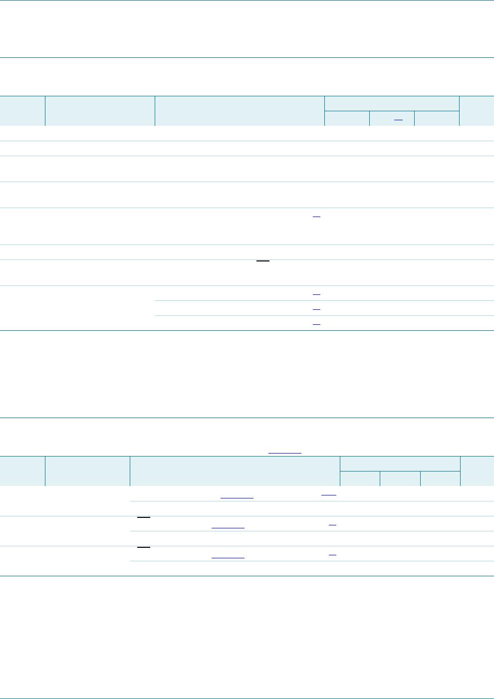
Table 3. Pin description
Symbol Pin Description
1OE
, 2OE 1, 7 output enable input
1A, 2A 2, 5 data input/output (A port)
1B, 2B 3, 6 data input/output (B port)
GND 4 ground (0 V)
V
CC
8 positive supply voltage
Table 4. Function selection
[1]
Input Input/output
nOE nA, nB
LnA = nB
HZ
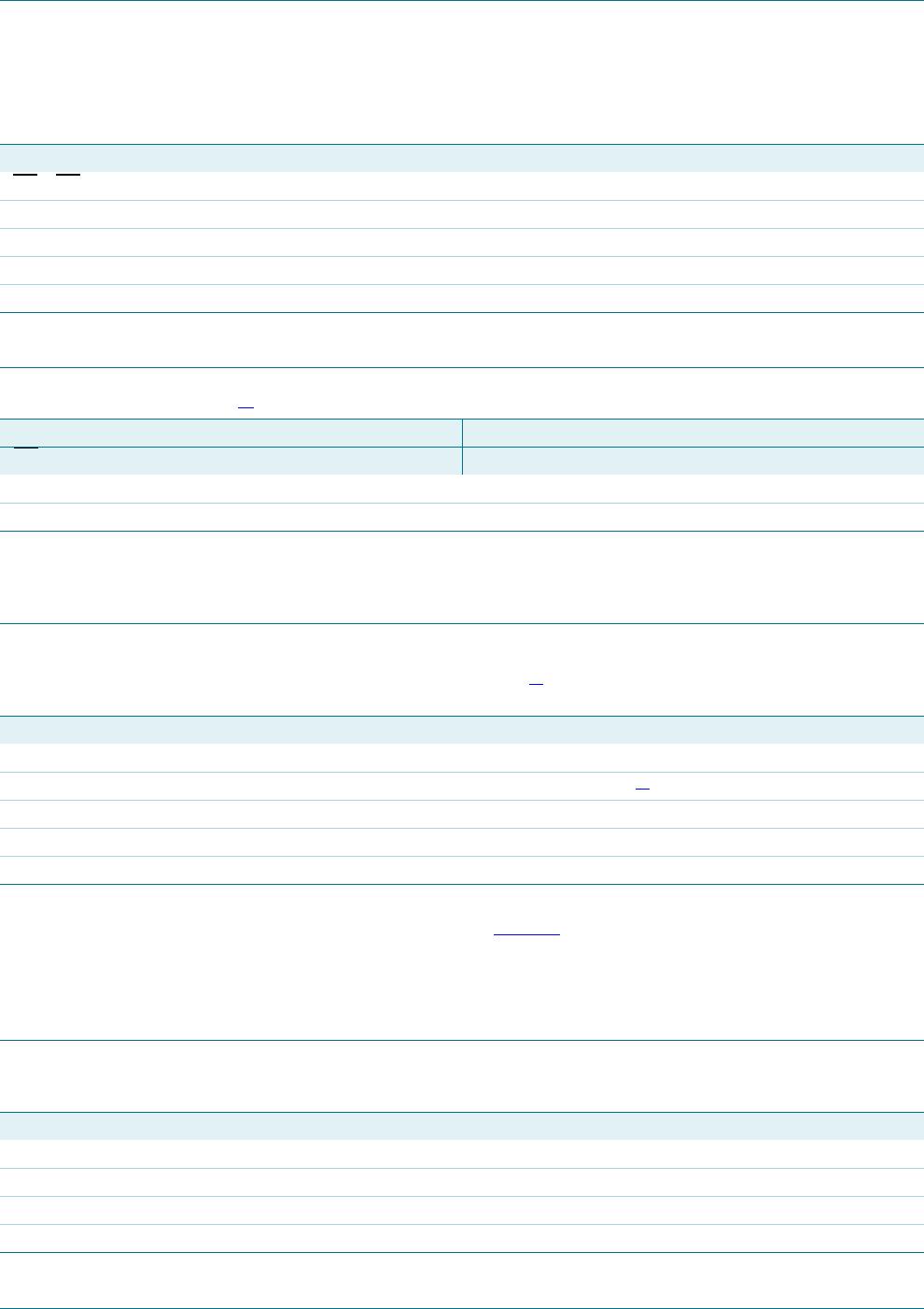
Table 5. Limiting values
In accordance with the Absolute Maximum Rating System (IEC 60134).
[1]
T
amb
=
40
C to +85
C, unless otherwise specified.
Symbol Parameter Conditions Min Max Unit
V
CC
supply voltage 0.5 +7.0 V
V
I
input voltage
[2]
0.5 +7.0 V
I
O
output current - 128 mA
I
IK
input clamping current V
I/O
=0V 50 - mA
T
stg
storage temperature 65 +150 C
Table 6. Operating conditions
All unused control inputs of the device must be held at V
CC
or GND to ensure proper device operation.
Symbol Parameter Conditions Min Typ Max Unit
V
CC
supply voltage 4.5 - 5.5 V
V
IH
HIGH-level input voltage 2.0 - - V
V
IL
LOW-level input voltage - - 0.8 V
T
amb
ambient temperature operating in free air 40 - +85 C