CBT3306 All information provided in this document is subject to legal disclaimers. © NXP B.V. 2012. All rights reserved.
Product data sheet Rev. 7 — 1 May 2012 6 of 14
NXP Semiconductors
CBT3306
Dual bus switch
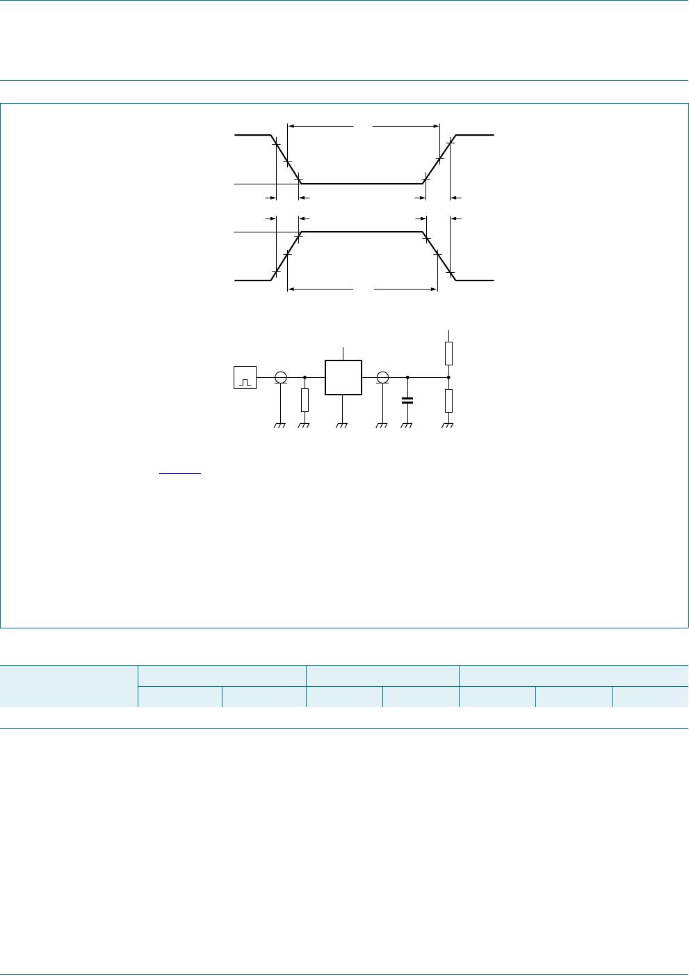
13. Test information
Test data is given in Table 10.
All input pulses are supplied by generators having the following characteristics: PRR 10 MHz; Z
o
=50.
The outputs are measured one at a time with one transition per measurement.
Definitions for test circuit:
R
L
= Load resistance.
C
L
= Load capacitance including jig and probe capacitance.
R
T
= Termination resistance should be equal to output impedance Z
o
of the pulse generator.
V
EXT
= External voltage for measuring switching times.
Fig 8. Test circuit for measuring switching times
V
M
V
M
t
W
t
W
10 %
90 %
0 V
V
I
V
I
negative
pulse
positive
pulse
0 V
V
M
V
M
90 %
10 %
t
f
t
r
t
r
t
f
001aae331
V
EXT
V
CC
V
I
V
O
DUT
C
L
R
T
R
L
R
L
G
Table 10. Test data
Supply voltage Input Load V
EXT
V
I
t
r
, t
f
C
L
R
L
t
PLH
, t
PHL
t
PLZ
, t
PZL
t
PHZ
, t
PZH
V
CC
= 5.0 V 0.5 V GND to 3.0 V 2.5 ns 50 pF 500 open 7.0 V open