LT1054/LT1054L
1
1954lfh
For more information www.linear.com/LT1054
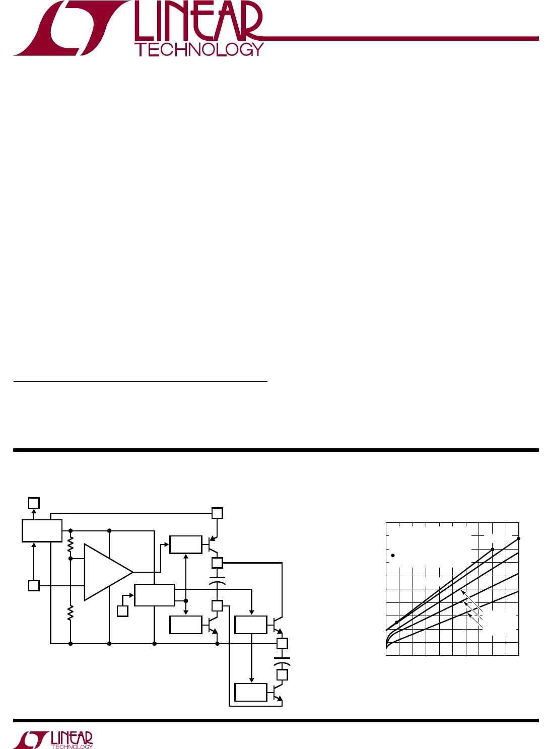
Block Diagram
Features Description
Switched-Capacitor Voltage
Converter with Regulator
The LT
®
1054 is a monolithic, bipolar, switched-capacitor
voltage converter and regulator. The LT1054 provides
higher output current than previously available converters
with significantly lower voltage losses. An adaptive switch
driver scheme optimizes efficiency over a wide range of
output currents. Total voltage loss at 100mA output current
is typically 1.1V. This holds true over the full supply voltage
range of 3.5V to 15V. Quiescent current is typically 2.5mA.
The LT1054 also provides regulation, a feature not previ
-
ously available in switched-capacitor voltage converters. By
adding an external resistive divider a regulated output can
be obtained. This output will be regulated against changes
in both input voltage and output current. The LT1054 can
also be shut down by grounding the feedback pin. Supply
current in shutdown is less than 100µA.
The internal oscillator of the LT1054 runs at a nominal
frequency of 25kHz. The oscillator pin can be used to ad
-
just the switching frequency or to externally synchronize
the L
T1054.
The L
T1054 is pin compatible with previous converters
such the LTC1044/ICL7660.
LT1054/LT1054 Voltage Loss
applications
Output Current: 100mA (LT1054)
125mA (LT1054L)
Reference and Error Amplifier for Regulation
Low Loss: 1.1V at 100mA
Operating Range: 3.5V to 15V (LT1054)
3.5V to 7V (LT1054L)
External Shutdown
External Oscillator Synchronization
Can Be Paralleled
Pin Compatible with the LTC
®
1044/ICL7660
Available in SW16 and SO-8 Packages
Voltage Inverter
Voltage Regulator
Negative Voltage Doubler
Positive Voltage Doubler
L, LT, LTC, LTM, Burst Mode, Linear Technology and the Linear logo are registered trademarks
and ThinSOT is a trademark of Linear Technology Corporation. All other trademarks are the
property of their respective owners.
REFERENCE
OSC
DRIVE DRIVE
DRIVE
DRIVE
OSC
CAP
GND
CAP
+
FEEDBACK/
SHUTDOWN
+
R
R
*EXTERNAL CAPACITORS
2.5V
6
1
4
3
–V
OUT
LT1054 • BD
5
2
8
7
Q
Q
V
REF
C
IN
*
V
IN
C
OUT
*
+
+
OUTPUT CURRENT (mA)
0
VOLTAGE LOSS (V)
1
2
50
1054 TA01•
0
25
75 100
125
T
J
= 125°C
T
J
= 25°C
T
J
= –55°C
LT1054
LT1054L
3.5V ≤ V
IN
≤ 15V (LT1054)
3.5V ≤ V
IN
≤ 7V (LT1054L)
C
IN
= C
OUT
= 100µF
INDICATES GUARANTEED
TEST POINT
LT1054/LT1054L
2
1054lfh
For more information www.linear.com/LT1054
aBsolute maximum ratings
Supply Voltage (Note 2)
LT1054 .................................................................16V
LT1054L .................................................................7V
Input Voltage
Pin 1 ................................................. 0V V
PIN1
V
+
Pin 3 (S Package) ............................. 0V V
PIN3
V
+
Pin 7 .............................................. 0V V
PIN7
V
REF
Pin 13 (S Package) ...................... 0V V
PIN13
V
REF
Operating Junction Temperature Range
LT1054C/LT1054LC .............................. 0°C to 100°C
LT1054I ............................................. 40°C to 100°C
LT1054M ............................................ 55°C to 125°C
(Note 1)
1
2
3
4
8
7
6
5
TOP VIEW
FB/SHDN
CAP
+
GND
CAP
V
+
OSC
V
REF
V
OUT
N8 PACKAGE
8-LEAD PLASTIC DIP
J8 PACKAGE
8-LEAD CERAMIC DIP
T
JMAX
= 125°C, θ
JA
= 130°C/W
1
2
3
4
8
7
6
5
TOP VIEW
V
+
OSC
V
REF
V
OUT
FB/SHDN
CAP
+
GND
CAP
S8 PACKAGE
8-LEAD PLASTIC SO
T
JMAX
= 125°C, θ
JA
= 120°C/W
SEE REGULATION AND CAPACITOR SELECTION SECTIONS
IN THE APPLICATIONS INFORMATION FOR IMPORTANT
INFORMATION ON THE S8 DEVICE
1
2
3
4
5
6
7
8
TOP VIEW
SW PACKAGE
16-LEAD PLASTIC SO
16
15
14
13
12
11
10
9
NC
NC
FB/SHDN
CAP
+
GND
CAP
NC
NC
NC
NC
V
+
OSC
V
REF
V
OUT
NC
NC
T
JMAX
= 125°C, θ
JA
= 150°C/W
pin conFiguration
orDer inFormation
LEAD FINISH TAPE AND REEL PART MARKING PACKAGE DESCRIPTION TEMPERATURE RANGE
LT1054CN8#PBF LT1054CN8 8-Lead Plastic DIP 0°C to 100°C
LT1054IN8#PBF LT1054IN8 8-Lead Plastic DIP –40°C to 100°C
LT1054MJ8 LT1054MJ8 8-Lead Ceramic DIP –55°C to 125°C
LT1054CS8#PBF LT1054CS8#TRPBF 1054 8-Lead Plastic SO 0°C to 100°C
LT1054LCS8#PBF LT1054LCS8#TRPBF 1054L 8-Lead Plastic SO 0°C to 100°C
LT1054IS8#PBF LT1054IS8#TRPBF 1054I 8-Lead Plastic SO –40°C to 100°C
LT1054CSW#PBF LT1054CSW#TRPBF LT1054CSW 16-Lead Plastic SO 0°C to 100°C
LT1054ISW#PBF LT1054ISW#TRPBF LT1054ISW 16-Lead Plastic SO –40°C to 100°C
LT1054CJ8#PBF OBSOLETE PART LT1054CJ8#TRPBF LT1054CJ8 8-Lead Ceramic DIP 0°C to 100°C
Consult LTC Marketing for parts specified with wider operating temperature ranges.
Consult LTC Marketing for information on non-standard lead based finish parts.
For more information on lead free part marking, go to: http://www
.linear.com/leadfree/
For more information on tape and reel specifications, go to: http://www.linear.com/tapeandreel/
Maximum Junction Temperature (Note 3)
LT1054C/LT1054LC ......................................... 125°C
LT1054I ............................................................. 125°C
LT1054M ........................................................... 150°C
Storage Temperature Range
J8, N8 and S8 Packages .................... 55°C to 150°C
S Package ......................................... 65°C to 150°C
Lead Temperature (Soldering, 10 sec) .................. 300°C
LT1054/LT1054L
3
1954lfh
For more information www.linear.com/LT1054
electrical characteristics
Note 1: Stresses beyond those listed under Absolute Maximum Ratings
may cause permanent damage to the device. Exposure to any Absolute
Maximum Rating condition for extended periods may affect device
reliability and lifetime.
Note 2: The absolute maximum supply voltage rating of 16V is for
unregulated circuits using LT1054. For regulation mode circuits using
LT1054 with V
OUT
≤ 15V at Pin 5 (Pin 11 on S package), this rating may be
increased to 20V. The absolute maximum supply voltage for LT1054L is 7V.
Note 3: The devices are guaranteed by design to be functional up to the
absolute maximum junction temperature.
Note 4: For voltage loss tests, the device is connected as a voltage inverter,
with pins 1, 6, and 7 (3, 12, and 13 S package) unconnected. The voltage
losses may be higher in other configurations.
The l denotes the specifications which apply over the full operating
temperature range, otherwise specifications are at T
A
= 25°C. (Note 7)
PARAMETER CONDITIONS MIN TYP MAX UNITS
Supply Current I
LOAD
= 0mA LT1054: V
IN
= 3.5V
V
IN
= 15V
l
l
2.5
3.0
4.0
5.0
mA
mA
LT1054L:
V
IN
= 3.5V
V
IN
= 7V
l
l
2.5
3.0
4.0
5.0
mA
mA
Supply Voltage Range L
T1054
LT1054L
l
l
3.5
3.5
15
7
V
V
Voltage Loss (V
IN
– |V
OUT
|) C
IN
= C
OUT
= 100µF Tantalum (Note 4)
I
OUT
= 10mA
I
OUT
= 100mA
I
OUT
= 125mA (LT1054L)
l
l
l
0.35
1.10
1.35
0.55
1.60
1.75
V
V
V
Output Resistance
I
OUT
= 10mA to 100mA (Note 5)
l
10 15 Ω
Oscillator Frequency LT1054: 3.5V ≤ V
IN
≤ 15V
LT1054L: 3.5V ≤ V
IN
≤ 7V
l
l
15
15
25
25
40
35
kHz
kHz
Reference Voltage I
REF
= 60µA, T
J
= 25°C
l
2.35
2.25
2.50 2.65
2.75
V
V
Regulated Voltage V
IN
= 7V, T
J
= 25°C, R
L
= 500Ω (Note 6) –4.70 –5.00 –5.20 V
Line Regulation LT1054: 7V ≤ V
IN
≤ 12V, R
L
= 500Ω (Note 6)
l
5 25 mV
Load Regulation V
IN
= 7V, 100Ω ≤ 500Ω (Note 6)
l
10 50 mV
Maximum Switch Current 300 mA
Supply Current in Shutdown V
PIN1
= 0V
l
100 200 µA
Note 5: Output resistance is defined as the slope of the curve, (V
OUT
vs
I
OUT
), for output currents of 10mA to 100mA. This represents the linear
portion of the curve. The incremental slope of the curve will be higher at
currents <10mA due to the characteristics of the switch transistors.
Note 6: All regulation specifications are for a device connected as a
positive-to-negative converter/regulator with R1 = 20k, R2 = 102.5k,
C1 = 0.002µF, (C1 = 0.05µF S package) C
IN
= 10µF tantalum, C
OUT
= 100µF
tantalum.
Note 7: The S8 package uses a different die than the H, J8, N8 and S
packages. The S8 device will meet all the existing data sheet parameters.
See Regulation and Capacitor Selection in the Applications Information
section for differences in application requirements.
LT1054IS8#PBF

Mfr. #:
Manufacturer:
Analog Devices / Linear Technology
Description:
Linear Voltage Regulators 100mA Sw Cap Volt Converter
Lifecycle:
New from this manufacturer.
Delivery:
DHL FedEx Ups TNT EMS
Payment:
T/T Paypal Visa MoneyGram Western Union