LT6000/LT6001/LT6002
600012fa
10
TYPICAL PERFOR A CE CHARACTERISTICS
UW
1.5V
0.25V
100µs/DIVA
V
= 1
V
S
= 1.8V, 0V
C
L
= 100pF
R
L
= 10k
60012 G29
20mV/DIV
10µs/DIVA
V
= 1
V
S
= ±2.5V
C
L
= 100pF
R
L
= 100k
60012 G30
Large-Signal Response Small-Signal Response
Total Supply Current
vs SHDN Pin Voltage (LT6001DD)
SHDN PIN VOLTAGE (V)
0
0
SUPPLY CURRENT BOTH AMPLIFIERS (µA)
10
30
40
50
0.4
0.8
1.0 1.8
60012 G31
20
0.2 0.6
1.2
1.4
1.6
V
S
= 1.8V, 0V
T
A
= 125°C
T
A
= –55°C
T
A
= 25°C
Total Supply Current
vs SHDN Pin Voltage (LT6001DD)
SHDN PIN VOLTAGE (V)
0
SUPPLY CURRENT BOTH AMPLIFIERS (µA)
20
40
60
10
30
50
–3 –1 1 3
60012 G32
5–4–5 –2 0 2 4
V
S
= ±5V
T
A
= 125°C
T
A
= –55°C
T
A
= 25°C
0V
V
SHDN
V
OUT
0V
500µs/DIVV
IN
= 1V
A
V
= 1
V
S
= 1.8V, 0V
R
L
= 100k
60012 G33
Shutdown Response
(LT6000/LT6001DD)
Large-Signal Response
4.5V
0.5V
100µs/DIVA
V
= 1
V
S
= 5V, 0V
C
L
= 100pF
R
L
= 10k
60012 G28
Supply Current
vs SHDN Pin Voltage (LT6000)
Supply Current
vs SHDN Pin Voltage (LT6000)
SHDN PIN VOLTAGE (V)
0
0
SUPPLY CURRENT (µA)
5
15
20
25
0.4
0.8
1.0 1.8
60012 G37
10
0.2 0.6
1.2
1.4
1.6
30
V
S
= 1.8V, 0V
T
A
= 125°C
T
A
= –55°C
T
A
= 25°C
SHDN PIN VOLTAGE (V)
0
SUPPLY CURRENT (µA)
10
20
30
5
15
25
–3 –1 1 3
60012 G34
5–4–5 –2 0 2 4
T
A
= 125°C
V
S
= ±5V
T
A
= –55°C
T
A
= 25°C
LT6000/LT6001/LT6002
11
600012fa
Q1
Q17
Q6
Q2
Q10
C1
Q3
IN
+
Q8Q19 Q20
R1
R8
7M
R6 R7
R2
30k
D3
V
+
V
+
V
R4 R5
IN
R3
30k
Q9
Q11
Q14
V
+
OUT
V
SHDN
V
Q15
CM
Q13
COMPLEMENTARY
DRIVE GENERATOR
Q12
Q4
Q5
Q7
Q16
Q18
APPLICATIO S I FOR ATIO
WUUU
Supply Voltage
The positive supply of the LT6000/LT6001/LT6002 should
be bypassed with a small capacitor (about 0.01µF) within
an inch of the pin. When driving heavy loads, an additional
4.7µF electrolytic capacitor should be used. When using
split supplies, the same is true for the negative supply pin.
Rail-to-Rail Characteristics
The LT6000/LT6001/LT6002 are fully functional for an
input signal range from the negative supply to the positive
supply. Figure 1 shows a simplified schematic of the
amplifier. The input stage consists of two differential
amplifiers, a PNP stage Q3/Q6 and an NPN stage Q4/Q5
that are active over different ranges of the input common
mode voltage. The PNP stage is active for common mode
voltages, V
CM
, between the negative supply to approxi-
mately 1V below the positive supply. As V
CM
moves closer
towards the positive supply, the transistor Q7 will steer
Q2’s tail current to the current mirror Q8/Q9, activating the
NPN differential pair. The PNP pair becomes inactive for
the rest of the input common mode range up to the
positive supply.
The second stage is a folded cascode and current mirror
that converts the input stage differential signals into a
single ended output. Capacitor C1 reduces the unity cross
frequency and improves the frequency stability without
degrading the gain bandwidth of the amplifier. The comple-
mentary drive generator supplies current to the output
transistors that swing from rail to rail.
Input
The input bias current depends on which stage is active.
The input bias current polarity depends on the input
common mode voltage. When the PNP stage is active, the
input bias currents flow out of the input pins. They flow in
the opposite direction when the NPN stage is active. The
offset error due to the input bias currents can be
minimized by equalizing the noninverting and inverting
source impedance.
Figure 1
SI PLIFIED SCHE ATIC
WW
LT6000/LT6001/LT6002
600012fa
12
APPLICATIO S I FOR ATIO
WUUU
The input offset voltage changes depending on which
input stage is active; input offset voltage is trimmed on
both input stages, and is guaranteed to be 600µV max in
the PNP stage. By trimming the input offset voltage of
both input stages, the input offset voltage over the entire
common mode range (CMRR) is typically 400µV, main-
taining the precision characteristics of the amplifier.
The input stage of the LT6000/LT6001/LT6002 incorpo-
rates phase reversal protection to prevent wrong polarity
outputs from occurring when the inputs are driven up to
2V below the negative rail. 30k protective resistors are
included in the input leads so that current does not
become excessive when the inputs are forced below V
or
when a large differential signal is applied. Input current
should be limited to 10mA when the inputs are driven
above the positive rail.
Output
The output of the
LT6000/
LT6001/LT6002 can swing to
within 30mV of the positive rail with no load and within
30mV of the negative rail with no load. When monitoring
input voltages within 30mV of the positive rail or within
30mV of the negative rail, gain should be taken to keep
the output from clipping. The
LT6000/
LT6001/LT6002
can typically source 10mA on a single 5V supply, sourc-
ing current is reduced to 4mA on a single 1.8V supply as
noted in the electrical characteristics.
The normally reverse-biased substrate diode from the
output to V
will cause unlimited currents to flow when the
output is forced below V
. If the current is transient and
limited to 100mA, no damage will occur.
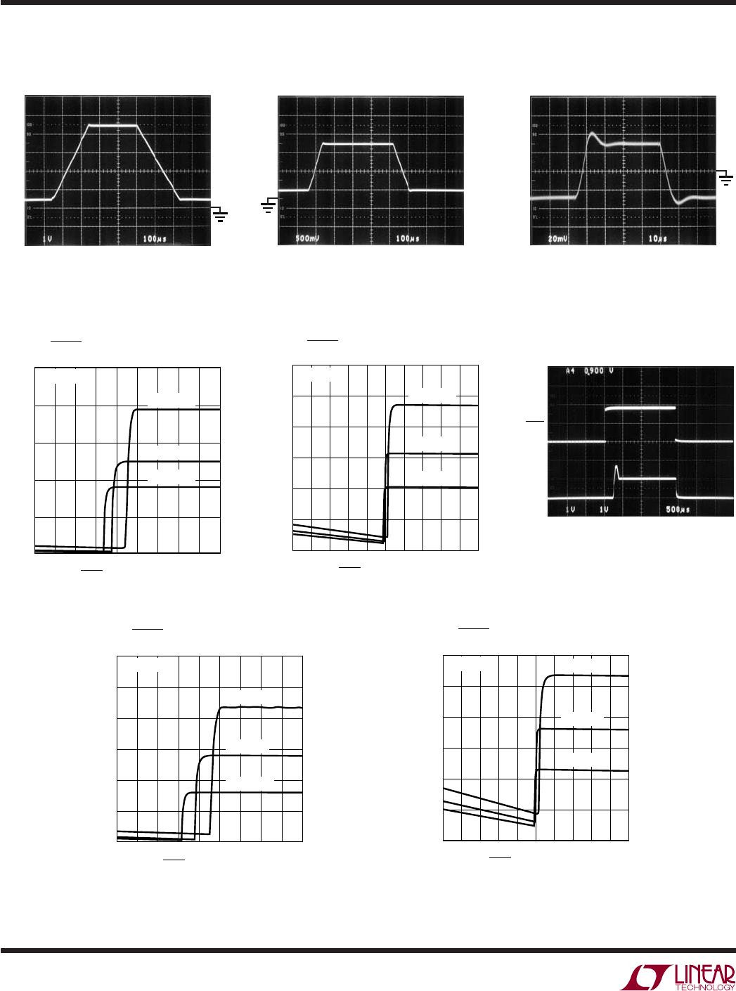
Start-Up and Output Saturation Characteristics
Micropower op amps are often not micropower during
start-up characteristics or during output saturation. This
can wreak havoc on limited current supplies, in the worst
case there may not be enough supply current available to
take the system up to nominal voltages. Also, when the
output saturates, the part may draw excessive current and
pull down the supplies, compromising rail-to-rail perfor-
mance. Figure 1 shows the start-up characteristics of the
LT6000/LT6001/LT6002 for three limiting cases. The cir-
cuits are shown in Figure 2. One circuit creates a positive
offset forcing the output to come up saturated high.
Another circuit creates a negative offset forcing the output
to come up saturated low, while the last circuit brings the
output up at 1/2 supply. In all cases, the supply current is
well controlled and is not excessive when the output is on
either rail.
SUPPLY VOLTAGE (V)
0
SUPPLY CURRENT PER AMPLIFIER (µA)
12
16
20
4
60012 F01
8
4
10
14
18
6
2
0
10.5
21.5
3 3.5 4.5
2.5
5
OUTPUT LOW
OUTPUT HIGH
OUTPUT AT V
S
/2
+
30mV
V
S
Output High
+
V
S
/2
V
S
60012 F02
Output at V
S
/2
+
30mV
V
S
Output Low
Figure 1. Start-Up Characteristics
Figure 2. Circuits for Start-Up Characteristics

LT6001IDD#PBF

Mfr. #:
Manufacturer:
Analog Devices Inc.
Description:
Precision Amplifiers 2x 1.8V, 13uA Prec R2R Op Amp
Lifecycle:
New from this manufacturer.
Delivery:
DHL FedEx Ups TNT EMS
Payment:
T/T Paypal Visa MoneyGram Western Union