LT6000/LT6001/LT6002
13
600012fa
APPLICATIO S I FOR ATIO
WUUU
The LT6000/LT6001/LT6002 outputs can swing to within
a respectable 30mV of each rail and draw virtually no
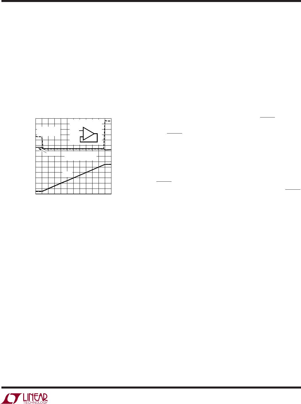
excessive supply current. Figure 3 compares the dual
LT6001 to a competitive part. Both op amps are in unity
gain and their outputs are driven into each rail. The supply
current is shown when the op amps are in linear operation
and when they are driven into each rail. As can be seen
from Figure 3, the supply current of the competitive part
increases 3-fold or 5-fold depending on which rail the
output goes to whereas the LT6001 draws virtually no
excessive current.
Gain
The open-loop gain is almost independent of load when
the output is sourcing current. This optimizes perfor-
mance in single supply applications where the load is
returned to ground. The typical performance curve of
Open-Loop Gain for various loads shows the details.
Shutdown
The single LT6000 and the 10-lead dual LT6001 include a
shutdown feature that disables the part reducing quies-
cent current and makes the output high impedance. The
devices can be shut down by bringing the SHDN pin within
0.3V of V
–
. The amplifiers are guaranteed to shut down if
the SHDN pin is brought within 0.3V of V
–
. The exact
switchover point will be a function of the supply voltage.
See the Typical Performance Characteristics curves Sup-
ply Current vs Shutdown Pin Voltage. When shut down the
total supply current is about 0.8µA and the output leakage
current is 20nA (V
–
≤ V
OUT
≤ V
+
). For normal operation the
SHDN pin should be tied to V
+
. It can be left floating,
however, parasitic leakage currents over 1µA at the SHDN
pin may inadvertently place the part into shutdown.
V
IN
(V)
–3
–3
V
OUT
(V)
I
CC
(µA)
–2
–1
0
4
2
–1
1
2
3
1
10
20
30
70
50
60
40
–2 0
3
60012 F03
V
IN
V
S
= ±2.5V, A
V
= 1
+
–
COMPETITIVE
PART
LT6001
V
OUT
SUPPLY CURRENT
PER AMPLIFIER
Figure 3. V
OUT
and I
CC
vs Input Voltage