IRLI540NPbF
2 2017-04-27
Notes:
Repetitive rating; pulse width limited by max. junction temperature. (See fig. 11)
Starting T
J
= 25°C, L = 1.9mH, R
G
= 25, I
AS
= 18A (See fig. 12)
I
SD
18A, di/dt 180A/µs, V
DD
V
(BR)DSS
, T
J
175°C.
Pulse width 300µs; duty cycle 2%.
t=60s, ƒ=60Hz
Uses IRL540N data and test conditions.
Electrical Characteristics @ T
J
= 25°C (unless otherwise specified)
Parameter Min. Typ. Max. Units Conditions
V
(BR)DSS
Drain-to-Source Breakdown Voltage 100 ––– ––– V V
GS
= 0V, I
D
= 250µA
V
(BR)DSS
/T
J
Breakdown Voltage Temp. Coefficient ––– 0.11 ––– V/°C Reference to 25°C, I
D
= 1mA
R
DS(on)
Static Drain-to-Source On-Resistance
––– ––– 0.044
V
GS
= 10V, I
D
= 12A
––– ––– 0.053 V
GS
= 5.0V, I
D
= 12A
––– ––– 0.063 V
GS
= 4.0V, I
D
= 10A
V
GS(th)
Gate Threshold Voltage 1.0 ––– 2.0 V V
DS
= V
GS
, I
D
= 250µA
gfs Forward Trans conductance 14 ––– ––– S V
DS
= 25V, I
D
= 18A
I
DSS
Drain-to-Source Leakage Current
––– ––– 25
µA
V
DS
= 100V, V
GS
= 0V
––– ––– 250 V
DS
= 80V,V
GS
= 0V,T
J
=150°C
I
GSS
Gate-to-Source Forward Leakage ––– ––– 100
nA
V
GS
= 16V
Gate-to-Source Reverse Leakage ––– ––– -100 V
GS
= -16V
Q
g
Total Gate Charge ––– ––– 74
nC
I
D
= 18A
Q
gs
Gate-to-Source Charge ––– ––– 9.4 V
DS
= 80V
Q
gd
Gate-to-Drain Charge ––– ––– 38
V
GS
= 5.0V , See Fig. 6 and 13
t
d(on)
Turn-On Delay Time ––– 11 –––
ns
V
DD
= 50V
t
r
Rise Time ––– 81 –––
I
D
= 18A
t
d(off)
Turn-Off Delay Time ––– 39 –––
R
G
= 5.0V
GS
= 5.0V
t
f
Fall Time ––– 62 –––
R
D
= 2.7See Fig. 10
L
D
Internal Drain Inductance ––– 4.5 –––
nH
Between lead,
6mm (0.25in.)
L
S
Internal Source Inductance ––– 7.5 –––
from package
and center of die contact
C
iss
Input Capacitance ––– 1800 –––
pF
V
GS
= 0V
C
oss
Output Capacitance ––– 350 ––– V
DS
= 25V
C
rss
Reverse Transfer Capacitance ––– 170 –––
ƒ = 1.0MHz, See Fig. 5
C
Drain to Sink Capacitance ––– 12 ––– ƒ = 1.0MHz
Source-Drain Ratings and Characteristics
Parameter Min. Typ. Max. Units Conditions
I
S
Continuous Source Current
––– ––– 23
A
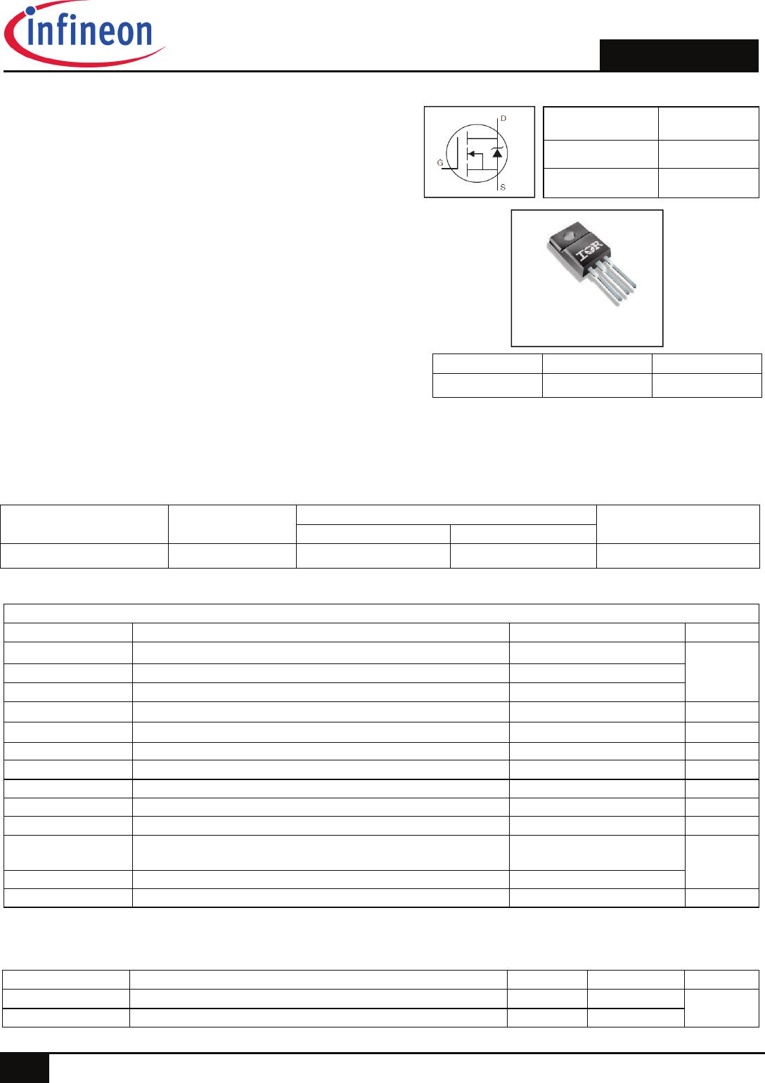
MOSFET symbol
(Body Diode)
showing the
I
SM
Pulsed Source Current
––– ––– 120
integral reverse
(Body Diode) p-n junction diode.
V
SD
Diode Forward Voltage ––– ––– 1.3 V T
J
= 25°C,I
S
= 18A,V
GS
= 0V
t
rr
Reverse Recovery Time ––– 190 290 ns
T
J
= 25°C ,I
F
= 18A
Q
rr
Reverse Recovery Charge ––– 1.1 1.7
C
di/dt = 100A/µs
t
on
Forward Turn-On Time
Intrinsic turn-on time is negligible (turn-on is dominated by L
S
+L
D
)