SMBus Digital Interface
From a software perspective, the MAX6698 appears as
a series of 8-bit registers that contain temperature mea-
surement data, alarm threshold values, and control bits.
A standard SMBus-compatible 2-wire serial interface is
used to read temperature data and write control bits
and alarm threshold data. The same SMBus slave
address also provides access to all functions.
The MAX6698 employs four standard SMBus protocols:
write byte, read byte, send byte, and receive byte
(Figure 2). The shorter receive byte protocol allows
quicker transfers, provided that the correct data regis-
ter was previously selected by a read byte instruction.
Use caution with the shorter protocols in multimaster
systems, since a second master could overwrite the
command byte without informing the first master. Figure
3 is the SMBus write timing diagram and Figure 4 is the
SMBus read timing diagram.
The remote diode 1 measurement channel provides 11
bits of data (1 LSB = 0.125°C). All other temperature-
measurement channels provide 8 bits of temperature
data (1 LSB = 1°C). The 8 most significant bits (MSBs)
can be read from the local temperature, remote tem-
perature, and thermistor registers. The remaining 3 bits
MAX6698
_______________________________________________________________________________________ 7
DXP1
DXN1
3-TO-1
MUX
INPUT
BUFFER
ADC
10/100µA
V
CC
CNT
COUNTER
VREF
COMMAND BYTE
REMOTE TEMPERATURES
LOCAL TEMPERATURES
REGISTER BANK
ALERT THRESHOLD
OVERT THRESHOLD
ALERT RESPONSE ADDRESS
ALU
DP
VREF1
SMBus
INTERFACE
MAX6698
SCL SDA
OVERT
ALERT
DXP3
DXN3
BUF1
BUF2
3-TO-1
MUX
R
EXT1
R
THER1
R
EXT2
R
THER1
R
EXT1
R
THER1
Figure 1. Internal Block Diagram
7-Channel Precision Remote-Diode, Thermistor,
and Local Temperature Monitor
MAX6698
for remote diode 1 can be read from the extended tem-
perature register. If extended resolution is desired, the
extended resolution register should be read first. This
prevents the most significant bits from being overwritten
by new conversion results until they have been read. If
the most significant bits have not been read within an
SMBus timeout period (nominally 25ms), normal updat-
ing continues. Table 1 shows themistor voltage data for-
mat. Table 2 shows the main temperature register (high
byte) data format. Table 3 shows the extended resolu-
tion temperature register (low byte) data format.
Diode Fault Detection
If a channel’s input DXP_ and DXN_ are left open, the
MAX6698 detects a diode fault. An open diode fault
does not cause either ALERT or OVERT to assert. A bit
in the status register for the corresponding channel is
set to 1 and the temperature data for the channel is
stored as all 1s (FFh). It takes approximately 4ms for
the MAX6698 to detect a diode fault. Once a diode fault
is detected, the MAX6698 goes to the next channel in
the conversion sequence. Depending on operating
conditions, a shorted diode may or may not cause
ALERT or OVERT to assert, so if a channel will not be
used, disconnect its DXP and DXN inputs.
Alarm Threshold Registers
There are 11 alarm threshold registers that store over-
temperature ALERT and OVERT threshold values.
Seven of these registers are dedicated to store one
local alert temperature threshold limit, three remote alert
temperature threshold limits, and three thermistor volt-
age threshold limits (see the
ALERT
Interrupt Mode sec-
tion). The remaining four registers are dedicated to
remote-diode channel 1, and three thermistor channels
1, 2, and 3 to store overtemperature threshold limits
(see the
OVERT
Overtemperature Alarm section).
Access to these registers is provided through the
SMBus interface.
7-Channel Precision Remote-Diode, Thermistor,
and Local Temperature Monitor
8 _______________________________________________________________________________________
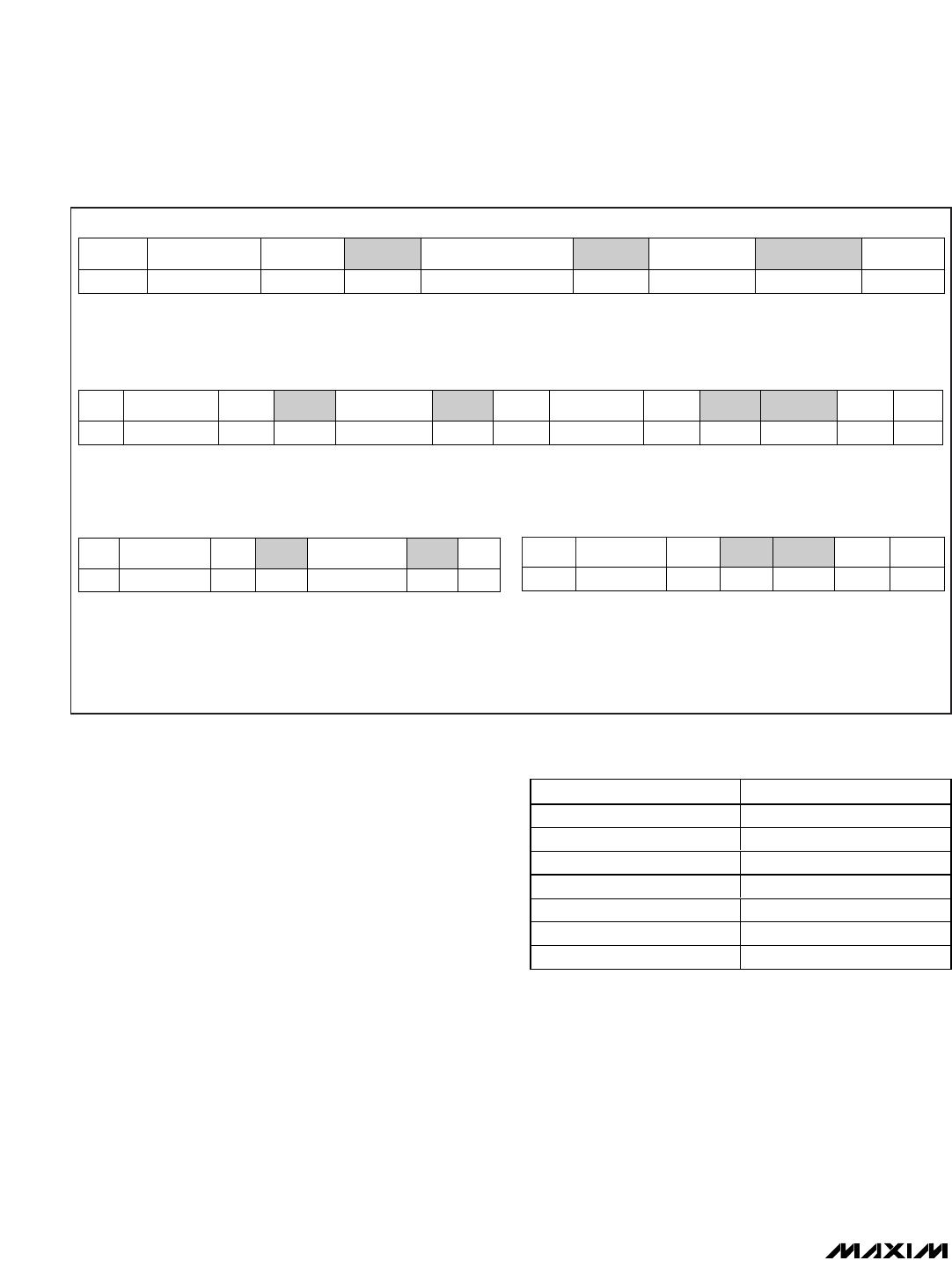
Figure 2. SMBus Protocols
Write Byte Format
Read Byte Format
Send Byte Format
Receive Byte Format
Slave Address: equiva-
lent to chip-select line of
a 3-wire interface
Command Byte: selects which
register you are writing to
Data Byte: data goes into the register
set by the command byte (to set
thresholds, configuration masks, and
sampling rate)
Slave Address: equiva-
lent to chip-select line
Command Byte: selects
which register you are
reading from
Slave Address: repeated
due to change in data-
flow direction
Data Byte: reads from
the register set by the
command byte
Command Byte: sends com-
mand with no data, usually
used for one-shot command
Data Byte: reads data from
the register commanded
by the last read byte or
write byte transmission;
also used for SMBus alert
response return address
S = Start condition Shaded = Slave transmission
P = Stop condition /// = Not acknowledged
S ADDRESS RD ACK DATA /// P
7 bits 8 bits
WRS ACK COMMAND ACK P
8 bits
ADDRESS
7 bits
P
1
ACKDATA
8 bits
ACKCOMMAND
8 bits
ACKWRADDRESS
7 bits
S
S ADDRESS WR ACK COMMAND ACK S ADDRESS
7 bits8 bits7 bits
RD ACK DATA
8 bits
/// P
V
REXT
DIGITAL OUTPUT
1.000 1100 1000
0.500 0110 0100
0.250 0011 0010
0.055 0000 1011
0.050 0000 1010
0.005 0000 0001
0.000 0000 0000
Table 1. Thermistor Voltage Data Format
MAX6698
_______________________________________________________________________________________ 9
7-Channel Precision Remote-Diode, Thermistor,
and Local Temperature Monitor
SMBCLK
A = START CONDITION
B = MSB OF ADDRESS CLOCKED INTO SLAVE
C = LSB OF ADDRESS CLOCKED INTO SLAVE
D = R/W BIT CLOCKED INTO SLAVE
AB CD
E
FG
HIJ
SMBDATA
t
SU:STA
t
HD:STA
t
LOW
t
HIGH
t
SU:DAT
t
SU:STO
t
BUF
LMK
E = SLAVE PULLS SMBDATA LINE LOW
F = ACKNOWLEDGE BIT CLOCKED INTO MASTER
G = MSB OF DATA CLOCKED INTO SLAVE
H = LSB OF DATA CLOCKED INTO SLAVE
I = MASTER PULLS DATA LINE LOW
J = ACKNOWLEDGE CLOCKED INTO SLAVE
K = ACKNOWLEDGE CLOCK PULSE
L = STOP CONDITION
M = NEW START CONDITION
Figure 3. SMBus Write Timing Diagram
SMBCLK
AB CD
E
FG H
I
J
K
SMBDATA
t
SU:STA
t
HD:STA
t
LOW
t
HIGH
t
SU:DAT
t
HD:DAT
t
SU:STO
t
BUF
A = START CONDITION
B = MSB OF ADDRESS CLOCKED INTO SLAVE
C = LSB OF ADDRESS CLOCKED INTO SLAVE
D = R/W BIT CLOCKED INTO SLAVE
E = SLAVE PULLS SMBDATA LINE LOW
L
M
F = ACKNOWLEDGE BIT CLOCKED INTO MASTER
G = MSB OF DATA CLOCKED INTO MASTER
H = LSB OF DATA CLOCKED INTO MASTER
I = MASTER PULLS DATA LINE LOW
J = ACKNOWLEDGE CLOCKED INTO SLAVE
K = ACKNOWLEDGE CLOCK PULSE
L = STOP CONDITION
M = NEW START CONDITION
Figure 4. SMBus Read Timing Diagram
TEMP (°C) DIGITAL OUTPUT
>127 0111 1111
127 0111 1111
126 0111 1110
25 00011001
0.00 0000 0000
<0.00 0000 0000
Diode fault (open) 1111 1111
Diode fault (short) 1111 1111 or 1110 1110
Table 2. Main Temperature Register (High
Byte) Data Format
TEMP (°C) DIGITAL OUTPUT
0 000X XXXX
+0.125 001X XXXX
+0.250 010X XXXX
+0.375 011X XXXX
+0.500 100X XXXX
+0.625 101X XXXX
+0.725 110X XXXX
+0.875 111X XXXX
Table 3. Extended Resolution
Temperature Register (Low Byte) Data
Format

MAX6698EE38+

Mfr. #:
Manufacturer:
Maxim Integrated
Description:
Board Mount Temperature Sensors 7-Ch Prec Therm Temp Monito
Lifecycle:
New from this manufacturer.
Delivery:
DHL FedEx Ups TNT EMS
Payment:
T/T Paypal Visa MoneyGram Western Union