NCP718ASN330T1G

© Semiconductor Components Industries, LLC, 2017
June, 2018 Rev. 5
1 Publication Order Number:
NCP718/D
NCP718
300 mA Low Iq, Wide Input
Voltage Low Dropout
Regulator
The NCP718 is 300 mA LDO Linear Voltage Regulator. It is a very
stable and accurate device with ultralow quiescent current
consumption (typ. 4 mA over the full temperature range) and a wide
input voltage range (up to 24 V). The regulator incorporates several
protection features such as Thermal Shutdown and Current Limiting.
Features
Operating Input Voltage Range: 2.5 V to 24 V
Fixed Voltage Options Available: 1.2 V to 5 V (upon request)
Adjustable Voltage Option from 1.2 V to 5 V
UltraLow Quiescent Current: typ. 4 mA over Temperature
±2% Accuracy Over Full Load, Line and Temperature Variations
PSRR: 60 dB at 1 kHz
Noise: typ. 36 mV
RMS
from 100 Hz to 100 kHz
Stable with Small 1 mF Ceramic Capacitor
Softstart to Reduce Inrush Current and Overshoots
Thermal Shutdown and Current Limit Protection
SOA Limiting for High Vin / High Iout – Static / Dynamic
Active Discharge Option Available (upon request)
Available in TSOT235 and WDFN6 2x2 mm Packages
These Devices are PbFree, Halogen Free/BFR Free and are RoHS
Compliant
Typical Applications
Wireless Chargers
Portable Equipment
Communication Systems
Figure 1. Typical Application Schematic
1
mF
Ceramic
NCP718
IN OUT
GND
C
OUT
C
IN
V
IN
V
OUT
1
mF
Ceramic
EN
OFF
ON
NC
www.onsemi.com
See detailed ordering and shipping information in the package
dimensions section on page 7 of this data sheet.
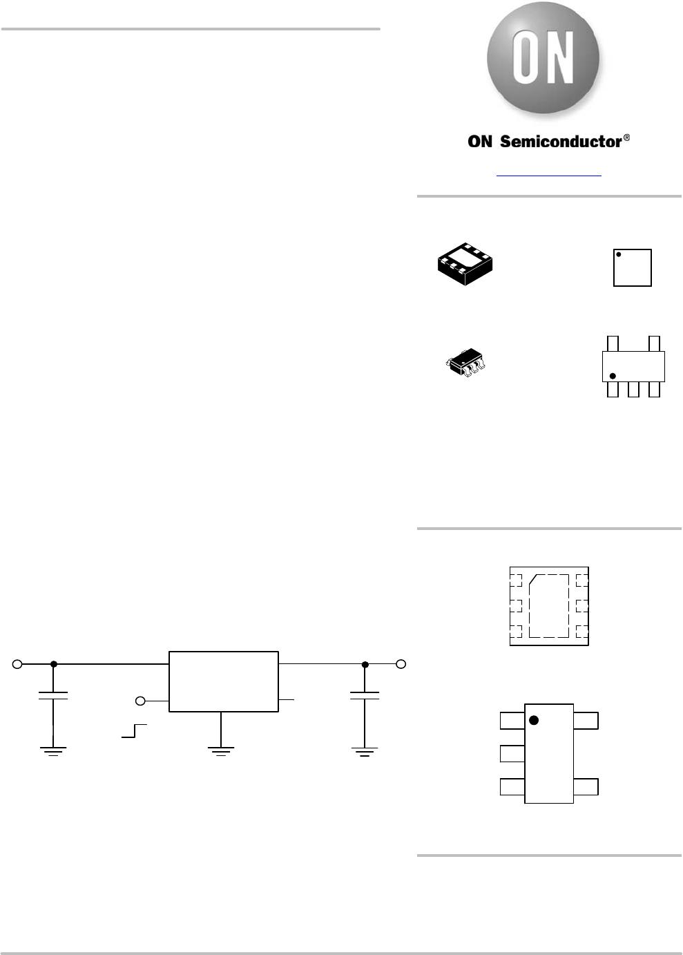
ORDERING INFORMATION
MARKING
DIAGRAMS
WDFN6
MT SUFFIX
CASE 511BR
PIN CONNECTIONS
WDFN6 2x2 mm
(Top View)
1
2
3
XX M
1
6
5
4
TSOT235
SN SUFFIX
CASE 419AE
1
XX MG
G
1
(Note: Microdot may be in either location)
XX = Specific Device Code
M = Date Code*
G = PbFree Package
XX = Specific Device Code
M = Date Code
TSOT235
(Top View)
1
*Date Code orientation and/or position may
vary depending upon manufacturing location.
IN
NC
EN
OUT
NC/ADJ
GND
IN
GND
EN
OUT
NC/ADJ
GND
NCP718
www.onsemi.com
2
Figure 2. Simplified Block Diagram
IN
THERMAL
SHUTDOWN
MOSFET
DRIVER WITH
CURRENT LIMIT
INTEGRATED
SOFTSTART
BANDGAP
REFERENCE
ENABLE
LOGIC
EN
OUT
GND
EN
* ACTIVE DISCHARGE
Version A only
IN
THERMAL
SHUTDOWN
MOSFET
DRIVER WITH
CURRENT LIMIT
INTEGRATED
SOFTSTART
BANDGAP
REFERENCE
ENABLE
LOGIC
EN
OUT
GND
EN
* ACTIVE DISCHARGE
Version A only
ADJ
Fixed Version
Adjustable Version
Table 1. PIN FUNCTION DESCRIPTION
Pin No.
(WDFN6)
Pin No.
(TSOT235)
Pin Name Description
6 1 IN Input pin. A small capacitor is needed from this pin to ground to assure stability.
3, EXP 2 GND Power supply ground.
4 3 EN Enable pin. Driving this pin high turns on the regulator. Driving EN pin low puts the regu-
lator into shutdown mode.
2 4 NC / ADJ Fixed Version: No connection. This pin can be tied to ground to improve thermal dissipa-
tion or left disconnected.
Adjustable Version: Feedback pin for setup output voltage. Use resistor divider for volt-
age selection.
1 5 OUT
Regulated output voltage pin. A small 1 mF ceramic capacitor is needed from this pin to
ground to assure stability.
5 N/C No connection. This pin can be tied to ground to improve thermal dissipation or left dis-
connected.
Table 2. ABSOLUTE MAXIMUM RATINGS
Rating Symbol Value Unit
Input Voltage (Note 1) V
IN
0.3 to 24 V
Enable Voltage V
EN
0.3 to V
IN+0.3
V
Output Voltage V
OUT
0.3 to V
IN+0.3
(max. 6) V
Output Short Circuit Duration t
SC
Indefinite s
Maximum Junction Temperature T
J(MAX)
150 °C
Storage Temperature T
STG
55 to 150 °C
ESD Capability, Human Body Model (Note 2) ESD
HBM
2000 V
ESD Capability, Charged Device Model (Note 2) ESD
CDM
1000 V
Stresses exceeding those listed in the Maximum Ratings table may damage the device. If any of these limits are exceeded, device functionality
should not be assumed, damage may occur and reliability may be affected.
1. Refer to ELECTRICAL CHARACTERISTICS and APPLICATION INFORMATION for Safe Operating Area.
2. This device series incorporates ESD protection and is tested by the following methods:
ESD Human Body Model tested per AECQ100002 (EIA/JESD22A114)
ESD Charged Device Model tested per EIA/JESD22C101, Field Induced Charge Model.
Latch up Current Maximum Rating tested per JEDEC standard: JESD78. Latchup is not guaranteed on ENABLE pin.
NCP718
www.onsemi.com
3
Table 3. THERMAL CHARACTERISTICS
Rating Symbol Value Unit
Thermal Characteristics, WDFN6, 2 mm x 2 mm
Thermal Resistance, JunctiontoAir
R
q
JA
65 °C/W
Thermal Characteristics, TSOT235
Thermal Resistance, JunctiontoAir
R
q
JA
235 °C/W
Table 4. ELECTRICAL CHARACTERISTICS -40°C T
J
125°C; V
IN
= 2.5 V or (V
OUT
+ 1.0 V), whatever is greater; I
OUT
= 1 mA,
C
IN
= C
OUT
= 1 mF, unless otherwise noted. Typical values are at T
J
= +25°C. (Note 3)
Parameter
Test Conditions Symbol Min Typ Max Unit
Operating Input Voltage V
IN
2.5 24 V
Output Voltage Accuracy
(fixed versions)
40°C T
J
125°C,
V
OUT
+ 1 V < V
IN
< 16 V,
0.1 mA < I
OUT
< 300 mA (Note 5)
V
OUT
< 1.8 V
V
OUT
3% +3%
V
V
OUT
1.8 V 2% +2%
Reference Voltage
40°C T
J
125°C,
V
OUT
+ 1 V < V
IN
< 16 V
V
ADJ
1.2 V
Reference Voltage Accuracy
40°C T
J
125°C,
V
OUT
+ 1 V < V
IN
< 16 V
V
OUT
2% +2% V
Line Regulation V
OUT
+ 1 V V
IN
16 V, Iout = 1 mA Reg
LINE
10 mV
Load Regulation I
OUT
= 0.1 mA to 300 mA Reg
LOAD
10 mV
Dropout voltage V
DO
= V
IN
– (V
OUT(NOM)
– 3%),
I
OUT
= 300 mA (Note 4)
2.1 V – 2.4 V
V
DO
480
mV
2.5 V 2.7 V 320 490
2.8 V 3.2 V 295 465
3.3 V – 4.9 V 275 440
5 V 240 380
Maximum Output Current V
IN
= V
OUT
+ 1 V (Note 5) I
LIM
300 800 mA
Disable Current V
EN
= 0 V, V
IN
= 5 V I
DIS
0.1 1.0
mA
Quiescent Current
I
OUT
= 0 mA, 40°C T
J
125°C
I
Q
4.0 8.0
mA
Ground current
I
OUT
= 10 mA
I
GND
50 mA
I
OUT
= 300 mA 300
Power Supply Rejection Ratio V
IN
= 3.5 V + 100 mVpp
V
OUT
= 2.5 V
I
OUT
= 1 mA, Cout = 1 mF
f = 1 kHz PSRR 60 dB
Output Noise Voltage V
OUT
= 1.2 V, I
OUT
= 10 mA
f = 100 Hz to 100 kHz
V
N
36
mV
rms
Enable Input Threshold Voltage
Voltage increasing V
EN_HI
1.2
V
Voltage decreasing V
EN_LO
0.4
ADJ Pin Current V
IN
= V
OUT
+ 1 V I
ADJ
0.1 1.0
mA
EN Pin Current V
EN
= 5.5 V I
EN
100 nA
Active Output Discharge
Resistance
V
IN
= 5.5 V, V
EN
= 0 V Rdis 100
W
Thermal Shutdown Temperature
(Note 6)
Temperature increasing from T
J
= +25°C T
SD
165 °C
Thermal Shutdown Hysteresis
(Note 6)
Temperature falling from T
SD
T
SDH
25 °C
Product parametric performance is indicated in the Electrical Characteristics for the listed test conditions, unless otherwise noted. Product
performance may not be indicated by the Electrical Characteristics if operated under different conditions.
3. Performance guaranteed over the indicated operating temperature range by design and/or characterization production tested at T
J
= T
A
=
25°C. Low duty cycle pulse techniques are used during testing to maintain the junction temperature as close to ambient as possible.
4. Voltage dropout for voltage variants below 2.1 V is given by minimum input voltage 2.5 V.
5. Respect SOA
6. Guaranteed by design and characterization.

NCP718ASN330T1G

Mfr. #:
Manufacturer:
ON Semiconductor
Description:
300 MA LOW IQ WIDE INPUT
Lifecycle:
New from this manufacturer.
Delivery:
DHL FedEx Ups TNT EMS
Payment:
T/T Paypal Visa MoneyGram Western Union