For free samples & the latest literature: http://www.maxim-ic.com, or phone 1-800-998-8800.
For small orders, phone 1-800-835-8769.
General Description
The MAX4661/MAX4662/MAX4663 quad analog switches
feature low on-resistance of 2.5 max. On-resistance is
matched between switches to 0.5 max and is flat
(0.5 max) over the specified signal range. Each
switch can handle Rail-to-Rail
®
analog signals. Off-
leakage current is only 5nA max at T
A
= +85°C. These
analog switches are ideal in low-distortion applications
and are the preferred solution over mechanical relays in
automatic test equipment or applications where current
switching is required. They have lower power require-
ments, use less board space, and are more reliable
than mechanical relays.
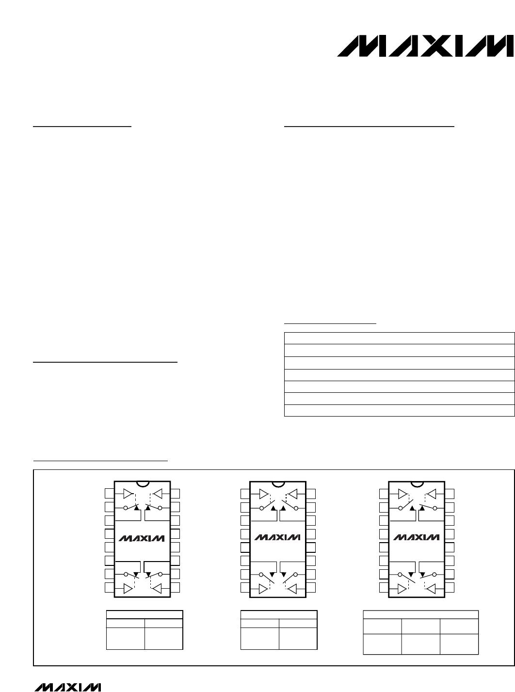
The MAX4661 has four normally closed (NC) switches,
and the MAX4662 has four normally open (NO) switches.
The MAX4663 has two NC and two NO switches, and fea-
tures guaranteed break-before-make switching.
These devices operate from a single +4.5V to +36V sup-
ply or from dual ±4.5V to ±20V supplies. A separate logic
supply pin guarantees TTL/CMOS-logic compatibility
when operating across the entire supply voltage range.
Applications
Reed Relay Replacement Avionics
Test Equipment ADC Systems
Communication Systems Sample-and-Hold Circuits
PBX, PABX Systems Data Acquisition Systems
Audio-Signal Routing
Features
Low On-Resistance (2.5max)
Guaranteed R
ON
Match Between Channels
(0.5 max)
Guaranteed R
ON
Flatness over Specified Signal
Range (0.5 max)
Rail-to-Rail Signal Handling
Guaranteed Break-Before-Make (MAX4663)
> 2kV ESD Protection per Method 3015.7
+4.5V to +36V Single-Supply Operation
±4.5V to ±20V Dual-Supply Operation
TTL/CMOS-Compatible Control Inputs
MAX4661/MAX4662/MAX4663
2.5
, Quad, SPST,
CMOS Analog Switches
________________________________________________________________
Maxim Integrated Products
1
19-1516; Rev 0; 7/99
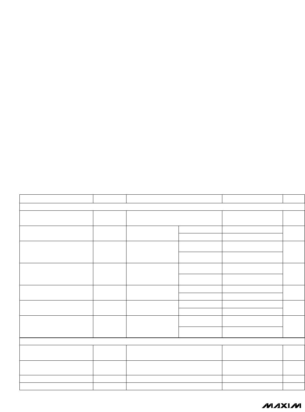
PART
MAX4661CAE
MAX4661CWE
MAX4661CPE 0°C to +70°C
0°C to +70°C
0°C to +70°C
TEMP. RANGE PIN-PACKAGE
16 SSOP
16 Wide SO
16 Plastic DIP
Ordering Information continued at end of data sheet.
Ordering Information
MAX4661EAE -40°C to +85°C 16 SSOP
MAX4661EWE -40°C to +85°C 16 Wide SO
MAX4661EPE -40°C to +85°C 16 Plastic DIP
SWITCHES SHOWN FOR LOGIC “0” INPUT
SSOP/SO/DIP
MAX4662
LOGIC SWITCH
0
1
OFF
ON
TOP VIEW
SSOP/SO/DIP
MAX4661
LOGIC SWITCH
0
1
ON
OFF
SSOP/SO/DIP
MAX4663
LOGIC
SWITCHES
1, 4
0
1
OFF
ON
SWITCHES
2, 3
ON
OFF
16
15
14
13
12
11
10
9
1
2
3
4
5
6
7
8
IN2
COM2
NC2
V+
V-
NO1
COM1
IN1
MAX4663
V
L
NC3
COM3
IN3
IN4
COM4
NO4
GND
16
15
14
13
12
11
10
9
1
2
3
4
5
6
7
8
IN2
COM2
NC2
V+
V-
NC1
COM1
IN1
MAX4661
V
L
NC3
COM3
IN3
IN4
COM4
NC4
GND
16
15
14
13
12
11
10
9
1
2
3
4
5
6
7
8
IN2
COM2
NO2
V+
V-
NO1
COM1
IN1
MAX4662
V
L
NO3
COM3
IN3
IN4
COM4
NO4
GND
Pin Configurations/Functional Diagrams/Truth Tables
Rail-to-Rail is a registered trademark of Nippon Motorola, Ltd.
MAX4661/MAX4662/MAX4663
2.5
, Quad, SPST,
CMOS Analog Switches
2 _______________________________________________________________________________________
ABSOLUTE MAXIMUM RATINGS
Stresses beyond those listed under “Absolute Maximum Ratings” may cause permanent damage to the device. These are stress ratings only, and functional
operation of the device at these or any other conditions beyond those indicated in the operational sections of the specifications is not implied. Exposure to
absolute maximum rating conditions for extended periods may affect device reliability.
V+ to GND..............................................................-0.3V to +44V
V- to GND ..............................................................+0.3V to -44V
V+ to V-...................................................................-0.3V to +44V
V
L
to GND .......................................(GND - 0.3V) to (V+ + 0.3V)
All Other Pins to GND (Note 1).............(V- - 0.3V) to (V+ + 0.3V)
Continuous Current (COM_, NO_, NC_) ........................±200mA
Peak Current (COM_, NO_, NC_)
(pulsed at 1ms, 10% duty cycle)................................ ±300mA
Continuous Power Dissipation (T
A
= +70°C)
SSOP (derate 7.1mW/°C above +70°C) .......................571mW
Wide SO (derate 9.52mW/°C above +70°C).................762mW
Plastic DIP (derate 10.53mW/°C above +70°C) ...........842mW
Operating Temperature Ranges
MAX466_C_E ......................................................0°C to +70°C
MAX466_E_E ....................................................-40°C to +85°C
Storage Temperature Range .............................-65°C to +150°C
Lead Temperature (soldering, 10sec) .............................+300°C
-5 5
-5 5
-20 20
T
A
= T
MIN
to T
MAX
V
T
A
= +25°C
V- V+
V
COM_,
V
NO_,
V
NC_
Input Voltage Range (Note 3)
IN_ = 0.8V, all others = 2.4V
IN_ = 2.4V, all others = 0.8V
I
COM_
= 10mA,
V
NO_
or V
NC_
= ±10V
T
A
= +25°C
T
A
= +25°C
T
A
= +25°C
CONDITIONS
0.8V
IN_L
Logic Input Voltage Low
0.1 0.5
R
ON
COM_ to NO_ or NC_
On-Resistance Match Between
Channels (Notes 3, 4)
1.7 2.5
R
ON
COM_ to NO or NC_
On-Resistance
V2.4V
IN_H
Logic Input Voltage High
-0.5 0.001 0.5I
IN_L
Input Current with Input Voltage
Low
µA-0.5 0.001 0.5I
IN_H
Input Current with Input Voltage
High
0.1 0.5
R
FLAT(ON)
COM_ to NO_ or NC_
On-Resistance Flatness
(Notes 3, 5)
nA
-0.5 0.01 0.5
I
NO_,
I
NC_
Off-Leakage Current
(NO_ or NC_) (Note 6)
nA
-0.5 0.01 0.5
I
COM_(OFF)
COM Off-Leakage Current
(Note 6)
nA
-1 0.01 1
I
COM_(ON)
COM On-Leakage Current
(Note 6)
UNITSMIN TYP MAXSYMBOLPARAMETER
I
COM_
= 10mA,
V
NO_
or V
NC_
= ±10V
I
COM_
= 10mA; V
NO_
or V
NC_
= -5V, 0, 5V
T
A
= +25°C
V
COM_
= ±10V,
V
NO_
or V
NC_
=
+
10V
V
COM_
= ±10V,
V
NO_
or V
NC_
=
+
10V
V
COM_
= ±10V,
V
NO_
or V
NC_
= ±10V
or floating
T
A
= +25°C
T
A
= T
MIN
to T
MAX
2.7
0.6
T
A
= T
MIN
to T
MAX
0.6
T
A
= T
MIN
to T
MAX
T
A
= T
MIN
to T
MAX
T
A
= T
MIN
to T
MAX
ELECTRICAL CHARACTERISTICS—Dual Supplies
(V+ = +15V, V- = -15V, V
L
= +5V, V
IN_H
= +2.4V, V
IN_L
= +0.8V, T
A
= T
MIN
to T
MAX
, unless otherwise noted. Typical values are at
T
A
= +25°C.) (Note 2)
µA
V
ANALOG SWITCH
LOGIC INPUT
Note 1: Signals on NC_, NO_, COM_, or IN_ exceeding V+ or V- will be clamped by internal diodes. Limit forward diode current to maximum
current rating.
MAX4661/MAX4662/MAX4663
2.5
, Quad, SPST,
CMOS Analog Switches
_______________________________________________________________________________________ 3
V
IN
= 0 or 5V µA
T
A
= +25°C
-0.5 0.001 0.5
I+Positive Supply Current
T
A
= +25°C
f = 1MHz, Figure 7
R
L
= 50, C
L
= 5pF, f = 1MHz,
Figure 6
T
A
= T
MIN
to T
MAX
-5 5
R
L
= 50, C
L
= 5pF, f = 1MHz,
Figure 5
V
COM_
= ±10V, Figure 3, T
A
= +25°C
V
IN
= 0 or 5V
T
A
= +25°C
f = 1MHz, Figure 7
CONDITIONS
V±4.5 ±20.0Power-Supply Range
pF
dB
f = 1MHz, Figure 8 pF250C
COM
On-Capacitance
55C
COM
COM_ Off-Capacitance
-0.5 0.001 0.5
I
L
Logic Supply Current
-0.5 0.001 0.5
I-Negative Supply Current
pFC
OFF
NC_ or NO_ Capacitance
-59V
CT
Crosstalk (Note 8)
dB-56V
ISO
Off-Isolation (Note 7)
ns530t
OPEN
Break-Before-Make Time
(MAX4663 only)
-0.5 0.001 0.5
I
GND
Ground Current
130 275
100 175
UNITSMIN TYP MAXSYMBOLPARAMETER
V
IN
= 0 or 5V
V
IN
= 0 or 5V
T
A
= +25°C
T
A
= T
MIN
to T
MAX
-5 5
-5 5
T
A
= T
MIN
to T
MAX
-5 5
ELECTRICAL CHARACTERISTICS—Dual Supplies (continued)
(V+ = +15V, V- = -15V, V
L
= +5V, V
IN_H
= +2.4V, V
IN_L
= +0.8V, T
A
= T
MIN
to T
MAX
, unless otherwise noted. Typical values are at
T
A
= +25°C.) (Note 2)
µA
µA
µA
T
A
= T
MIN
to T
MAX
55
ns
400
t
ON
Turn-On Time
V
COM_
= ±10V,
Figure 2
ns
300
t
OFF
Turn-Off Time
V
COM_
= ±10V,
Figure 2
C
L
= 1.0nF, V
GEN
= 0, R
GEN
= 0,
Figure 4
pC300QCharge Injection
POWER SUPPLY
SWITCH DYNAMIC CHARACTERISTICS
T
A
= +25°C
T
A
= T
MIN
to T
MAX
T
A
= +25°C
T
A
= T
MIN
to T
MAX

MAX4662EAE+

Mfr. #:
Manufacturer:
Maxim Integrated
Description:
Analog Switch ICs 2.5Ohm Quad SPST Analog Switch
Lifecycle:
New from this manufacturer.
Delivery:
DHL FedEx Ups TNT EMS
Payment:
T/T Paypal Visa MoneyGram Western Union