MAX4661/MAX4662/MAX4663
2.5
Ω
, Quad, SPST,
CMOS Analog Switches
_______________________________________________________________________________________ 7
NAME FUNCTION
MAX4661
1, 16, 9, 8
IN1, IN2,
IN3, IN4
Logic-Control Digital Inputs
2, 15,
10, 7
COM1, COM2,
COM3, COM4
Analog Switch Common Terminals
3, 14, 11, 6
NC1, NC2,
NC3, NC4
Analog Switch Normally Closed Terminals
4 V-
Negative Analog Supply-Voltage Input. Connect to GND for single-
supply operation.
— NC2, NC3 Analog Switch Normally Closed Terminals
— NO1, NO4 Analog Switch Normally Open Terminals
—
NO1, NO2,
NO3, NO4
Analog Switch Normally Open Terminals
13 V+ Positive Analog Supply Input
12 V
L
Logic-Supply Input
5 GND Ground
Pin Description
MAX4662
1, 16, 9, 8
2, 15,
10, 7
—
4
—
—
3, 14, 11, 6
13
12
5
MAX4663
1, 16, 9, 8
PIN
2, 15,
10, 7
—
4
14, 11
3, 6
—
13
12
5
Applications Information
Overvoltage Protection
Proper power-supply sequencing is recommended for
all CMOS devices. Do not exceed the absolute maxi-
mum ratings because stresses beyond the listed rat-
ings can cause permanent damage to the devices.
Always sequence V+ on first, then V-, followed by the
logic inputs, NO, or COM. If power-supply sequencing
is not possible, add two small-signal diodes (D1, D2)
in series with the supply pins and a Schottky diode
between V+ and V
L
for overvoltage protection (Figure
1). Adding diodes reduces the analog signal range to
one diode drop below V+ and one diode drop above V-,
but does not affect the devices’ low switch resistance
and low leakage characteristics. Device operation is
unchanged, and the difference between V+ and V-
should not exceed 44V.
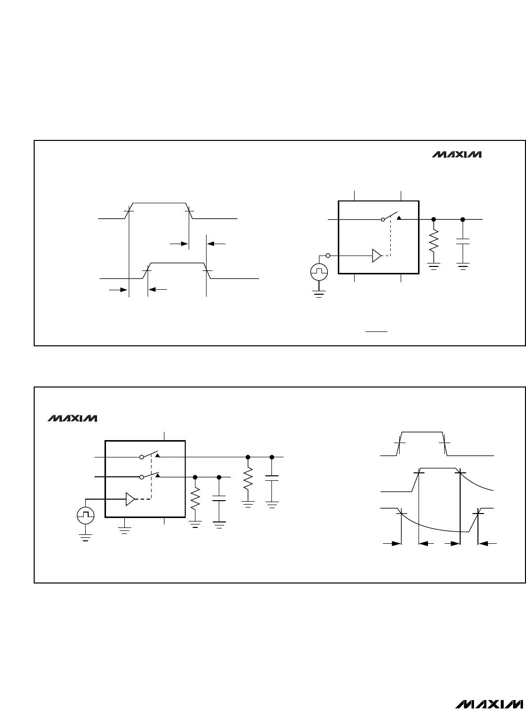
Off-Isolation at High Frequencies
In 50Ω systems, the high-frequency on-response of
these parts extends from DC to above 100MHz with a
typical loss of -2dB. When the switch is turned off, how-
ever, it behaves like a capacitor and off-isolation
decreases with increasing frequency. (Above 300MHz,
the switch actually passes more signal turned off than
turned on.) This effect is more pronounced with higher
source and load impedances.
Above 5MHz, circuit board layout becomes critical and
it becomes difficult to characterize the response of the
switch independent of the circuit. The graphs shown in
the
Typical Operating Characteristics
were taken using
a 50Ω source and load connected with BNC connec-
tors to a circuit board deemed “average”; that is,
designed with isolation in mind, but not using stripline
or other special RF circuit techniques. For critical appli-
cations above 5MHz, use the MAX440, MAX441, and
MAX442, which are fully characterized up to 160MHz.