3.2 Solder paste
1. Halide-free flux qualification ROL0 according to ANSI/J-STD-004.
2.
“No clean” solder paste is recommended.
3.
Offers a high tack force to resist component movement during high speed.
4. Use solder paste with fine particles: powder particle size 20-45 µm.
3.3 Placement
1. Manual positioning is not recommended.
2.
It is recommended to use the lead recognition capabilities of the placement system, not the outline centering
3.
Standard tolerance of ±0.05 mm is recommended.
4. 3.5 N placement force is recommended. Too much placement force can lead to squeezed out solder paste
and cause solder joints to short. Too low placement force can lead to insufficient contact between package
and solder paste that could cause open solder joints or badly centered packages.
5. To improve the package placement accuracy, a bottom side optical control should be performed with a high
resolution tool.
6. For assembly, a perfect supporting of the PCB (all the more on flexible PCB) is recommended during solder
paste printing, pick and place and reflow soldering by using optimized tools.
3.4 PCB design preference
1. To control the solder paste amount, the closed via is recommended instead of open vias.
2.
The position of tracks and open vias in the solder area should be well balanced. A symmetrical layout is
recommended, to avoid any tilt phenomena caused by asymmetrical solder paste due to solder flow away
.
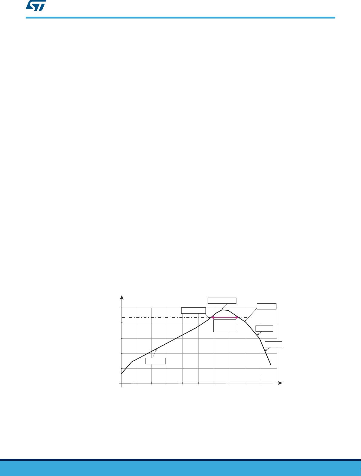
3.5 Reflow profile
Figure 15. ST ECOP
ACK
®
recommended soldering reflow profile for PCB mounting
250
0
50
100
150
200
240210180150120906030 300270
-6 °C/s
240-245 °C
2 - 3 °C/s
Temperature (°C)
-2 °C/s
-3 °C/s
Time (s)
0.9 °C/s
60 sec
(90 max)
Note: Minimize air convection currents in the reflow oven to avoid component movement.
ESDA22P150-1U3M
Solder paste
DS12572 - Rev 1
page 9/12