Data Sheet ADuM3300/ADuM3301
Rev. D | Page 17 of 20
APPLICATION INFORMATION
PC BOARD LAYOUT
The ADuM3300/ADuM3301 digital isolator requires no external
interface circuitry for the logic interfaces. Power supply
bypassing is strongly recommended at the input and output
supply pins (see Figure 14). Bypass capacitors are most
conveniently connected between Pin 1 and Pin 2 for V
DD1
and
between Pin 15 and Pin 16 for V
DD2
. The capacitor value should
be between 0.01 μF and 0.1 μF. The total lead length between
both ends of the capacitor and the input power supply pin
should not exceed 20 mm. Bypassing between Pin 1 and Pin 8
and between Pin 9 and Pin 16 should be considered unless the
ground pair on each package side is connected close to the
package.
V
DD1
GND
1
V
IA
V
IB
V
IC/OC
NC
V
E1
GND
1
V
DD2
GND
2
V
OA
V
OB
V
OC/IC
NC
V
E2
GND
2
05984-015
Figure 14. Recommended Printed Circuit Board Layout
In applications involving high common-mode transients, care
should be taken to ensure that board coupling across the
isolation barrier is minimized. Furthermore, the board layout
should be designed such that any coupling that does occur
equally affects all pins on a given component side. Failure to
ensure this could cause voltage differentials between pins
exceeding the device’s absolute maximum ratings, thereby
leading to latch-up or permanent damage.
See the AN-1109 Application Note for board layout guidelines.
SYSTEM-LEVEL ESD CONSIDERATIONS AND
ENHANCEMENTS
System-level ESD reliability (for example, per IEC 61000-4-x) is
highly dependent on system design, which varies widely by
application. The ADuM3300/ADuM3301 incorporate many
enhancements to make ESD reliability less dependent on system
design. The enhancements include
ESD protection cells added to all input/output interfaces.
Key metal trace resistances reduced using wider geometry
and paralleling of lines with vias.
The SCR effect inherent in CMOS devices minimized by
use of guarding and isolation technique between PMOS
and NMOS devices.
Areas of high electric field concentration eliminated using
45° corners on metal traces.
Supply pin overvoltage prevented with larger ESD clamps
between each supply pin and its respective ground.
While the ADuM3300/ADuM3301 improve system-level ESD
reliability, they are no substitute for a robust system-level
design. See Application Note AN-793 ESD/Latch-Up
Considerations with iCoupler Isolation Products for detailed
recommendations on board layout and system-level design.
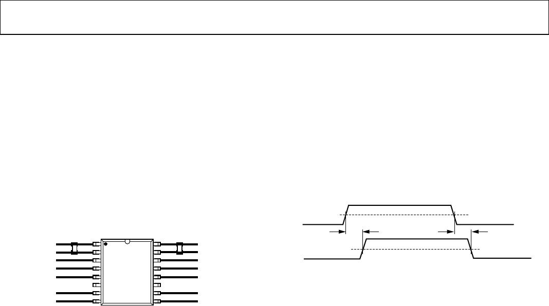
PROPAGATION DELAY-RELATED PARAMETERS
Propagation delay is a parameter that describes the time it takes
a logic signal to propagate through a component. The propagation
delay to a logic low output can differ from the propagation
delay to a logic high.
INPUT (
IX
)
OUTPUT (V
OX
)
t
PLH
t
PHL
50%
50%
05984-016
Figure 15. Propagation Delay Parameters
Pulse width distortion is the maximum difference between
these two propagation delay values and is an indication of how
accurately the input signal’s timing is preserved.
Channel-to-channel matching refers to the maximum amount
the propagation delay differs between channels within a single
ADuM3300/ADuM3301 component.
Propagation delay skew refers to the maximum amount the
propagation delay differs between multiple ADuM3300/
ADuM3301 components operating under the same conditions.
DC CORRECTNESS AND MAGNETIC FIELD IMMUNITY
Positive and negative logic transitions at the isolator input cause
narrow (~1 ns) pulses to be sent to the decoder via the transformer.
The decoder is bistable and is, therefore, either set or reset by
the pulses, indicating input logic transitions. In the absence of
logic transitions at the input for more than ~1 μs, a periodic set
of refresh pulses indicative of the correct input state is sent to
ensure dc correctness at the output. If the decoder receives no
internal pulses of more than about 5 μs, the input side is
assumed to be unpowered or nonfunctional, in which case the
isolator output is forced to a default state (see Table 11) by the
watchdog timer circuit.
The limitation on the ADuM3300/ADuM3301 magnetic field
immunity is set by the condition in which induced voltage in the
transformer’s receiving coil is sufficiently large to either falsely
set or reset the decoder. The following analysis defines the
conditions under which this can occur. The 3 V operating
condition of the ADuM3300/ADuM3301 are examined because
it represents the most susceptible mode of operation.