74AUP1T17
Low-power buffer with voltage-level translator
Rev. 1 — 28 November 2017 Product data sheet
1 General description
The 74AUP1T17 provides the single buffer function. This device ensures a very low static
and dynamic power consumption across the entire V
CC
range from 2.3 V to 3.6 V.
The 74AUP1T17 is designed for logic-level translation applications with input switching
levels that accept 1.8 V low-voltage CMOS signals, while operating from either a single
2.5 V or 3.3 V supply voltage.
The wide supply voltage range ensures normal operation as battery voltage drops from
3.6 V to 2.3 V.
This device is fully specified for partial power-down applications using I
OFF
. The I
OFF
circuitry disables the output, preventing the damaging backflow current through the
device when it is powered down.
Schmitt trigger inputs make the circuit tolerant to slower input rise and fall times across
the entire V
CC
range.
2 Features and benefits
Wide supply voltage range from 2.3 V to 3.6 V
High noise immunity
ESD protection:
HBM JESD22-A114F Class 3A exceeds 5000 V
CDM JESD22-C101E exceeds 1000 V
Low static power consumption; I
CC
= 1.5 μA (maximum)
Latch-up performance exceeds 100 mA per JESD 78 Class II
Inputs accept voltages up to 3.6 V
Low noise overshoot and undershoot < 10 % of V
CC
I
OFF
circuitry provides partial power-down mode operation
Multiple package options
Specified from -40 °C to +85 °C and -40 °C to +125 °C
Nexperia
74AUP1T17
Low-power buffer with voltage-level translator
74AUP1T17 All information provided in this document is subject to legal disclaimers. © Nexperia B.V. 2017. All rights reserved.
Product data sheet Rev. 1 — 28 November 2017
2 / 15
3 Ordering information
Table 1. Ordering information
PackageType number
Temperature
range
Name Description Version
74AUP1T17GW -40 °C to +125 °C TSSOP5 plastic thin shrink small outline package; 5 leads;
body width 1.25 mm
SOT353-1
74AUP1T17GX -40 °C to +125 °C X2SON5 plastic thermal enhanced extremely thin small outline
package; no leads; 5 terminals; body 0.8 x 0.8 x 0.35 mm
SOT1226
4 Marking
Table 2. Marking
Type number Marking code
[1]
74AUP1T17GW 57
74AUP1T17GX 57
[1] The pin 1 indicator is located on the lower left corner of the device, below the marking code.
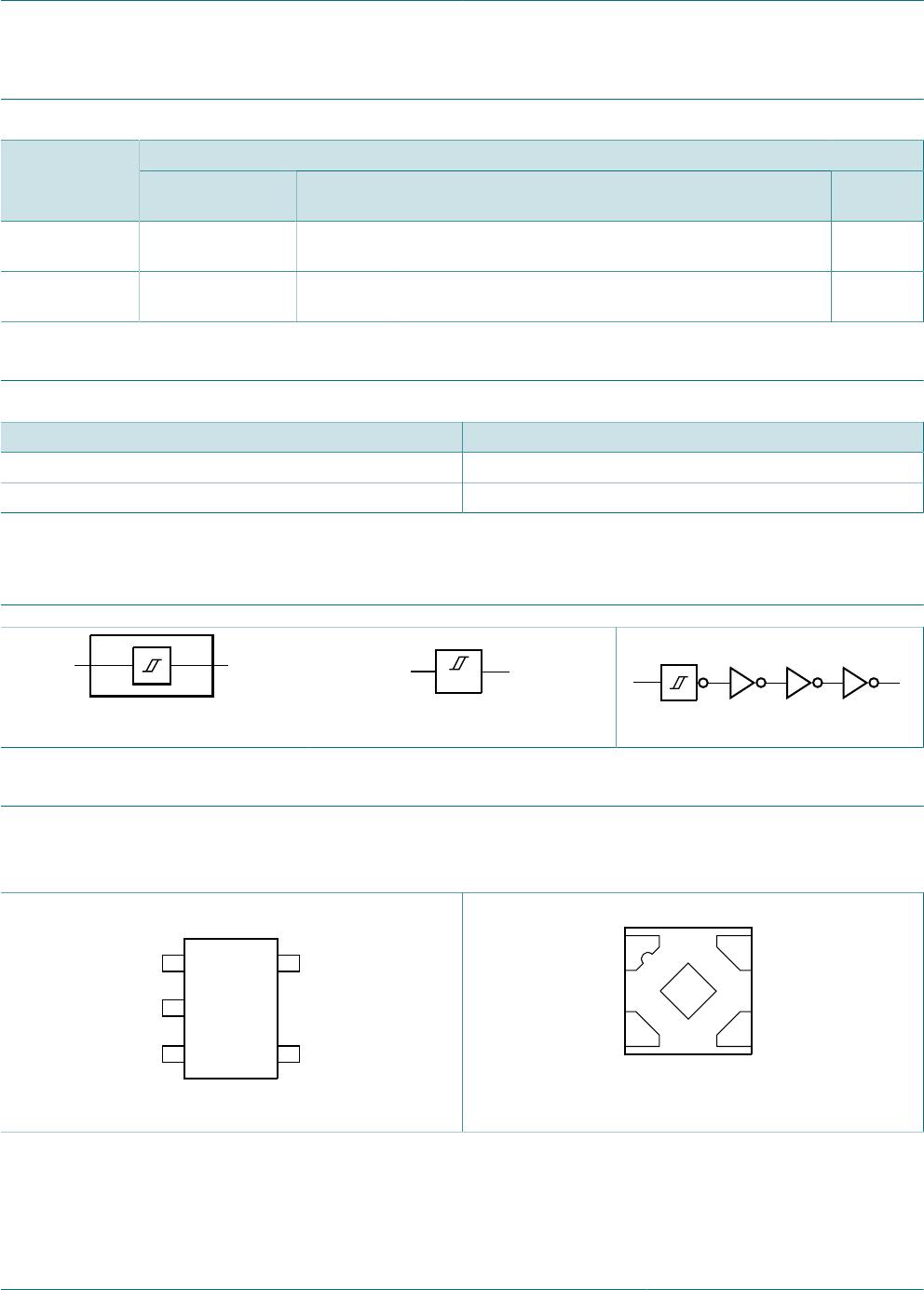
5 Functional diagram
mnb150
A Y
2
4
Figure 1. Logic symbol
2 4
mnb151
Figure 2. IEC logic symbol
mnb152
A
Y
Figure 3. Logic diagram
6 Pinning information
6.1 Pinning
74AUP1T17
n.c. V
CC
A
GND Y
aaa-027771
1
2
3
5
4
Figure 4. Pin configuration SOT353-1
n.c. V
CC
GND
1
3
2
5
4
A
Y
aaa-027772
Transparent top view
74AUP1T17
Figure 5. Pin configuration SOT1226 (X2SON5)
Nexperia
74AUP1T17
Low-power buffer with voltage-level translator
74AUP1T17 All information provided in this document is subject to legal disclaimers. © Nexperia B.V. 2017. All rights reserved.
Product data sheet Rev. 1 — 28 November 2017
3 / 15
6.2 Pin description
Table 3. Pin description
Symbol Pin Description
n.c. 1 not connected
A 2 data input
GND 3 ground (0 V)
Y 4 data output
V
CC
5 supply voltage
7 Functional description
Table 4. Function table
[1]
Input Output
A Y
L L
H H
[1] H = HIGH voltage level;
L = LOW voltage level.
8 Limiting values
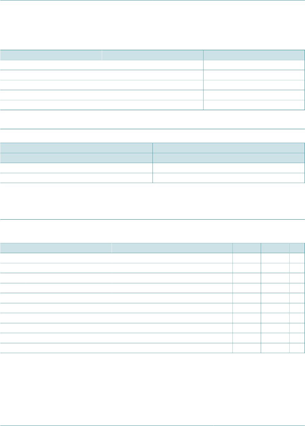
Table 5. Limiting values
In accordance with the Absolute Maximum Rating System (IEC 60134). Voltages are referenced to GND (ground = 0 V).
Symbol Parameter Conditions Min Max Unit
V
CC
supply voltage -0.5 +4.6 V
I
IK
input clamping current V
I
< 0 V -50 - mA
V
I
input voltage
[1]
-0.5 +4.6 V
I
OK
output clamping current V
O
< 0 V -50 - mA
V
O
output voltage Active mode and Power-down mode
[1]
-0.5 +4.6 V
I
O
output current V
O
= 0 V to V
CC
- ±20 mA
I
CC
supply current - 50 mA
I
GND
ground current -50 - mA
T
stg
storage temperature -65 +150 °C
P
tot
total power dissipation T
amb
= -40 °C to +125 °C
[2]
- 250 mW
[1] The minimum input and output voltage ratings may be exceeded if the input and output current ratings are observed.
[2] For TSSOP5 packages: above 87.5 °C the value of P
tot
derates linearly with 4.0 mW/K.
For X2SON5 packages: above 118 °C the value of P
tot
derates linearly with 7.8 mW/K.

74AUP1T17GXH

Mfr. #:
Manufacturer:
Nexperia
Description:
Translation - Voltage Levels 74AUP1T17GX/SOT1226/X2SON5
Lifecycle:
New from this manufacturer.
Delivery:
DHL FedEx Ups TNT EMS
Payment:
T/T Paypal Visa MoneyGram Western Union

Products related to this Datasheet