Nexperia
74AUP1T17
Low-power buffer with voltage-level translator
74AUP1T17 All information provided in this document is subject to legal disclaimers. © Nexperia B.V. 2017. All rights reserved.
Product data sheet Rev. 1 — 28 November 2017
7 / 15
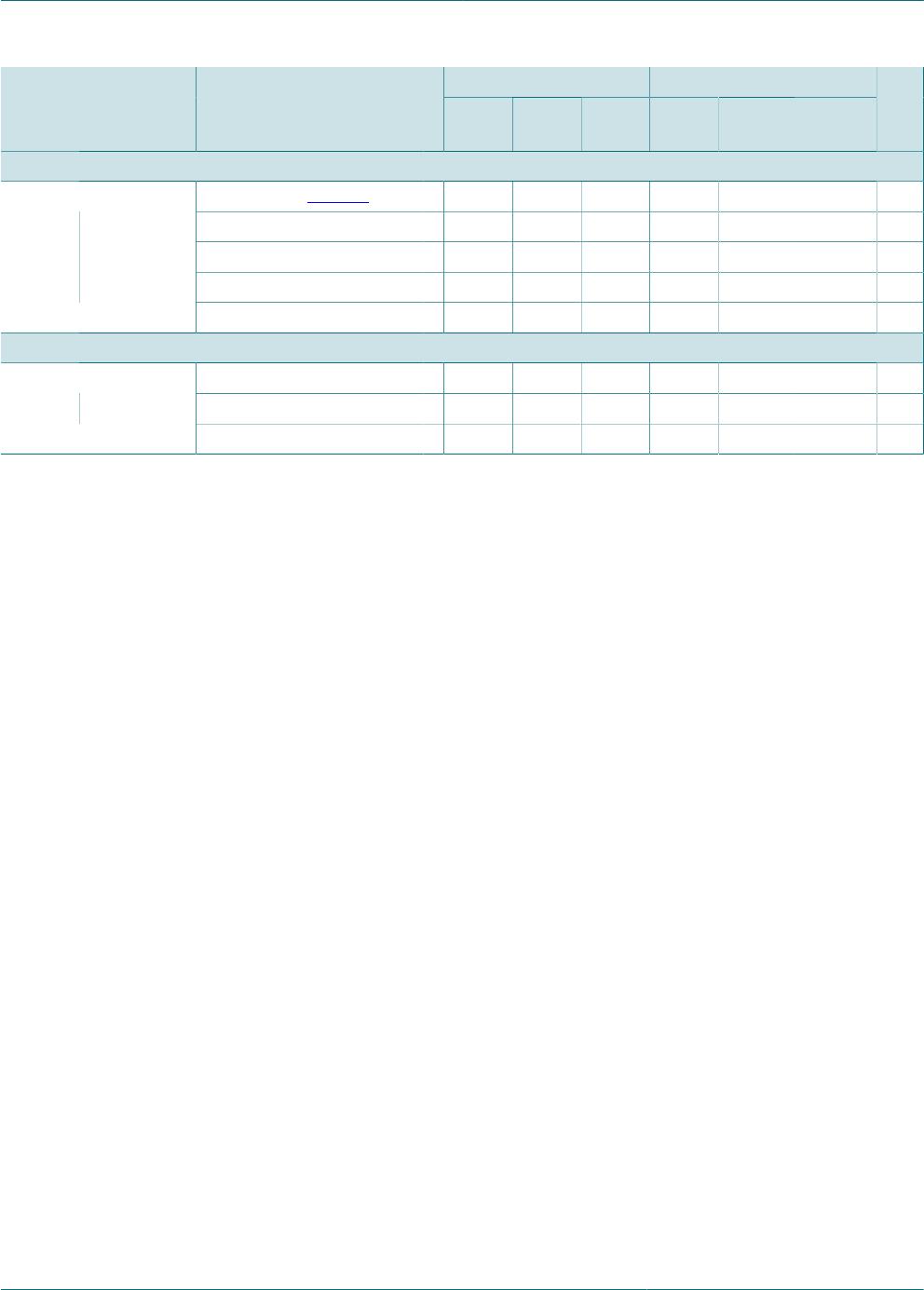
11 Dynamic characteristics
Table 8. Dynamic characteristics
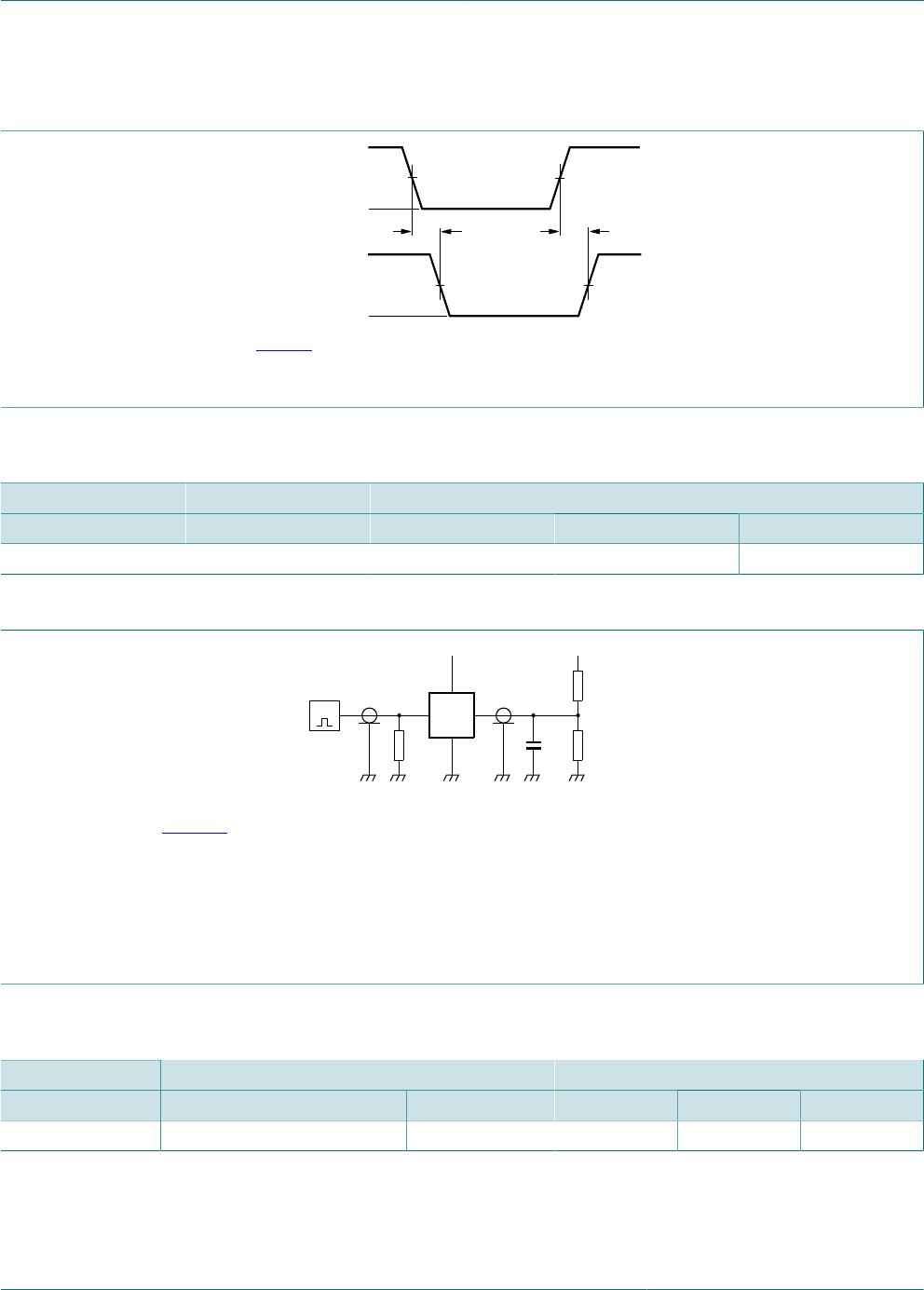
Voltages are referenced to GND (ground = 0 V); for test circuit see Figure 7.
25 °C -40 °C to +125 °CSymbol Parameter Conditions
Min Typ
[1]
Max Min Max
(85 °C)
Max
(125 °C)
Unit
V
CC
= 2.3 V to 2.7 V; V
I
= 1.65 V to 1.95 V
A, B to Y; see Figure 6
[2]
C
L
= 5 pF 2.0 3.2 4.9 0.5 6.8 7.5 ns
C
L
= 10 pF 2.4 3.8 5.6 1.0 7.9 8.7 ns
C
L
= 15 pF 2.7 4.3 6.1 1.0 8.7 9.6 ns
t
pd
propagation
delay
C
L
= 30 pF 3.6 5.4 7.6 1.5 10.8 11.9 ns
V
CC
= 2.3 V to 2.7 V; V
I
= 2.3 V to 2.7 V
A, B to Y; see Figure 6
[2]
C
L
= 5 pF 1.6 3.1 5.0 0.5 6.0 6.6 ns
C
L
= 10 pF 2.0 3.7 5.7 1.0 7.1 7.9 ns
C
L
= 15 pF 2.3 4.1 6.3 1.0 7.9 8.7 ns
t
pd
propagation
delay
C
L
= 30 pF 3.2 5.3 7.8 1.5 10.0 11.0 ns
V
CC
= 2.3 V to 2.7 V; V
I
= 3.0 V to 3.6 V
A, B to Y; see Figure 6
[2]
C
L
= 5 pF 1.2 2.8 4.5 0.5 5.5 6.1 ns
C
L
= 10 pF 1.7 3.4 5.1 1.0 6.5 7.2 ns
C
L
= 15 pF 2.0 3.9 5.7 1.0 7.4 8.2 ns
t
pd
propagation
delay
C
L
= 30 pF 2.8 5.0 7.2 1.5 9.5 10.5 ns
V
CC
= 3.0 V to 3.6 V; V
I
= 1.65 V to 1.95 V
A, B to Y; see Figure 6
[2]
C
L
= 5 pF 1.8 2.7 3.7 0.5 8.0 8.8 ns
C
L
= 10 pF 2.2 3.2 4.4 1.0 8.5 9.4 ns
C
L
= 15 pF 2.7 3.7 5.0 1.0 9.1 10.1 ns
t
pd
propagation
delay
C
L
= 30 pF 3.5 4.9 6.3 1.5 9.8 10.8 ns
V
CC
= 3.0 V to 3.6 V; V
I
= 2.3 V to 2.7 V
A, B to Y; see Figure 6
[2]
C
L
= 5 pF 1.4 2.6 3.8 0.5 5.3 5.9 ns
C
L
= 10 pF 1.9 3.1 4.5 1.0 6.1 6.8 ns
C
L
= 15 pF 2.2 3.6 5.1 1.0 6.8 7.5 ns
t
pd
propagation
delay
C
L
= 30 pF 3.0 4.8 6.6 1.5 8.5 9.4 ns
Nexperia
74AUP1T17
Low-power buffer with voltage-level translator
74AUP1T17 All information provided in this document is subject to legal disclaimers. © Nexperia B.V. 2017. All rights reserved.
Product data sheet Rev. 1 — 28 November 2017
8 / 15
25 °C -40 °C to +125 °CSymbol Parameter Conditions
Min Typ
[1]
Max Min Max
(85 °C)
Max
(125 °C)
Unit
V
CC
= 3.0 V to 3.6 V; V
I
= 3.0 V to 3.6 V
A, B to Y; see Figure 6
[2]
C
L
= 5 pF 1.1 2.5 4.0 0.5 4.7 5.2 ns
C
L
= 10 pF 1.6 3.1 4.5 1.0 5.7 6.3 ns
C
L
= 15 pF 1.9 3.6 5.1 1.0 6.2 6.9 ns
t
pd
propagation
delay
C
L
= 30 pF 2.7 4.7 6.6 1.5 7.8 8.6 ns
T
amb
= 25 °C
f
i
= 1 MHz; V
I
= GND to V
CC
[3]
V
CC
= 2.3 V to 2.7 V - 4 - - - - pF
C
PD
power
dissipation
capacitance
V
CC
= 3.0 V to 3.6 V - 5 - - - - pF
[1] All typical values are measured at nominal V
CC
.
[2] t
pd
is the same as t
PLH
and t
PHL
[3] C
PD
is used to determine the dynamic power dissipation (P
D
in μW).
P
D
= C
PD
x V
CC
2
x f
i
x N + Σ(C
L
x V
CC
2
x f
o
) where:
f
i
= input frequency in MHz;
f
o
= output frequency in MHz;
C
L
= output load capacitance in pF;
V
CC
= supply voltage in V;
N = number of inputs switching;
Σ(C
L
x V
CC
2
x f
o
) = sum of the outputs.
Nexperia
74AUP1T17
Low-power buffer with voltage-level translator
74AUP1T17 All information provided in this document is subject to legal disclaimers. © Nexperia B.V. 2017. All rights reserved.
Product data sheet Rev. 1 — 28 November 2017
9 / 15
11.1 Waveforms and test circuit
mnb153
t
PHL
t
PLH
V
M
V
M
A input
Y output
GND
V
I
V
OH
V
OL
Measurement points are given in Table 9
V
OL
and V
OH
are typical output voltage levels that occur with the output load.
Figure 6. Input A and B to output Y propagation delay times
Table 9. Measurement points
Supply voltage Output Input
V
CC
V
M
V
M
V
I
t
r
= t
f
2.3 V to 3.6 V 0.5 × V
CC
0.5 × V
I
1.65 V to 3.6 V ≤ 3.0 ns
001aac521
DUT
R
T
V
I
V
O
V
EXT
V
CC
R
L
5 kΩ
C
L
G
Test data is given in Table 10.
Definitions for test circuit:
R
L
= Load resistance.
C
L
= Load capacitance including jig and probe capacitance.
R
T
= Termination resistance should be equal to the output impedance Zo of the pulse generator.
V
EXT
= External voltage for measuring switching times.
Figure 7. Test circuit for measuring switching times
Table 10. Test data
Supply voltage Load V
EXT
V
CC
C
L
R
L
[1]
t
PLH
, t
PHL
t
PZH
, t
PHZ
t
PZL
, t
PLZ
2.3 V to 3.6 V 5 pF, 10 pF, 15 pF and 30 pF 5 kΩ or 1 MΩ open GND 2 × V
CC
[1] For measuring enable and disable times R
L
= 5 kΩ.
For measuring propagation delays, setup and hold times and pulse width R
L
= 1 MΩ.

74AUP1T17GXH

Mfr. #:
Manufacturer:
Nexperia
Description:
Translation - Voltage Levels 74AUP1T17GX/SOT1226/X2SON5
Lifecycle:
New from this manufacturer.
Delivery:
DHL FedEx Ups TNT EMS
Payment:
T/T Paypal Visa MoneyGram Western Union

Products related to this Datasheet