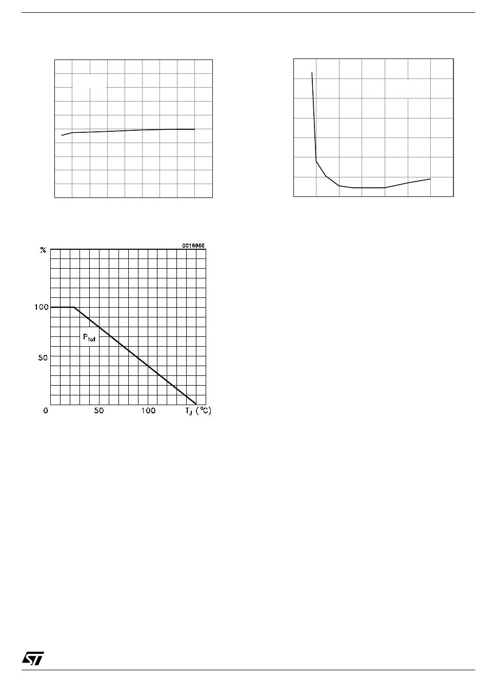
10/19
VNB35NV04 / VNP35NV04 / VNV35NV04 / VNW35NV04
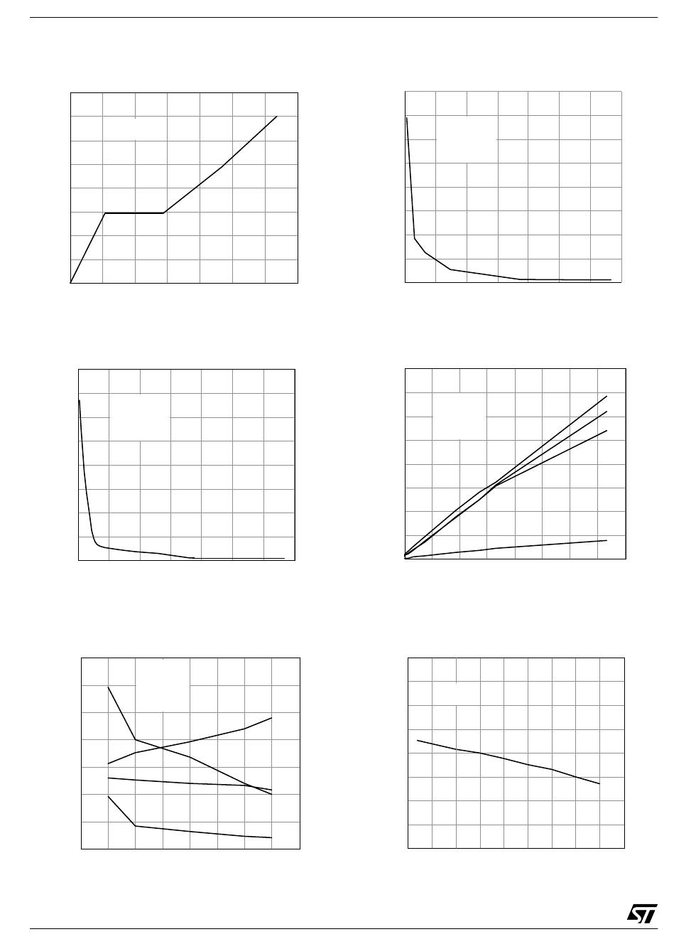
Turn Off Drain-Source Voltage Slope
Switching Time Resistive Load
0 150 300 450 600 750 900 1050
Rg (Ohm)
0
20
40
60
80
100
120
140
160
dV/dt (V/us)
Vin=3.5V
Vdd=15V
Id=15A
0 300 600 900 1200 1500 1800 2100 2400
Rg (Ohm)
0
5
10
15
20
25
30
35
40
T (us)
Vdd=15V
Id=15A
Rg=4.7ohm
td(off)
tf
tr
td(on)
Input Voltage Vs. Input Charge
Turn off drain source voltage slope
0 25 50 75 100 125 150 175
Qg (nC)
0
1
2
3
4
5
6
7
8
Vin (V)
Vds=12V
Id=15A
0 150 300 450 600 750 900 1050
Rg (Ohm)
0
20
40
60
80
100
120
140
160
dV/dt (V/us)
Vin=5V
Vdd=15V
Id=15A
3 3.5 4 4.5 5 5.5 6 6.5 7
Vin (V)
0
250
500
750
1000
1250
1500
1750
T (ns)
Vdd=15V
Id=15A
Rg=4.7ohm
td(off)
tf
tr
td(on)
-50 -25 0 25 50 75 100 125 150 175
Tc (ºC)
0
0.25
0.5
0.75
1
1.25
1.5
1.75
2
Vinth (V)
Vds=Vin
Id=1mA
Switching Time Resistive Load
Normalized Input Threshold Voltage Vs.
Temperature
11/19
VNB35NV04 / VNP35NV04 / VNV35NV04 / VNW35NV04
Step Response Current Limit
-50 -25 0 25 50 75 100 125 150 175
Tc (ºC)
0
10
20
30
40
50
60
70
80
90
100
Ilim (A)
Vin=6V
Vds=13V
Current Limit Vs. Junction Temperature
0 5 10 15 20 25 30 35
Vdd (V)
40
60
80
100
120
140
160
180
Tdlim (us)
Vin=6V
Derating Curve
12/19
VNB35NV04 / VNP35NV04 / VNV35NV04 / VNW35NV04
DIM.
mm. inch
MIN. TYP MAX. MIN. TYP. MAX.
A 4.40 4.60 0.173 0.181
C 1.23 1.32 0.048 0.051
D 2.40 2.72 0.094 0.107
E 0.49 0.70 0.019 0.027
F 0.61 0.88 0.024 0.034
F1 1.14 1.70 0.044 0.067
F2 1.14 1.70 0.044 0.067
G 4.95 5.15 0.194 0.203
G1 2.4 2.7 0.094 0.106
H2 10.0 10.40 0.393 0.409
L2 16.4 0.645
L4 13.0 14.0 0.511 0.551
L5 2.65 2.95 0.104 0.116
L6 15.25 15.75 0.600 0.620
L7 6.2 6.6 0.244 0.260
L9 3.5 3.93 0.137 0.154
M 2.6 0.102
DIA. 3.75 3.85 0.147 0.151
TO-220 MECHANICAL DATA

VNV35NV0413TR

Mfr. #:
Manufacturer:
STMicroelectronics
Description:
Power Switch ICs - Power Distribution N-Ch 40V 30A OmniFET
Lifecycle:
New from this manufacturer.
Delivery:
DHL FedEx Ups TNT EMS
Payment:
T/T Paypal Visa MoneyGram Western Union

Products related to this Datasheet