5/19
VNB35NV04 / VNP35NV04 / VNV35NV04 / VNW35NV04
PROTECTION FEATURES
During normal operation, the INPUT pin is
electrically connected to the gate of the internal
power MOSFET through a low impedance path.
The device then behaves like a standard power
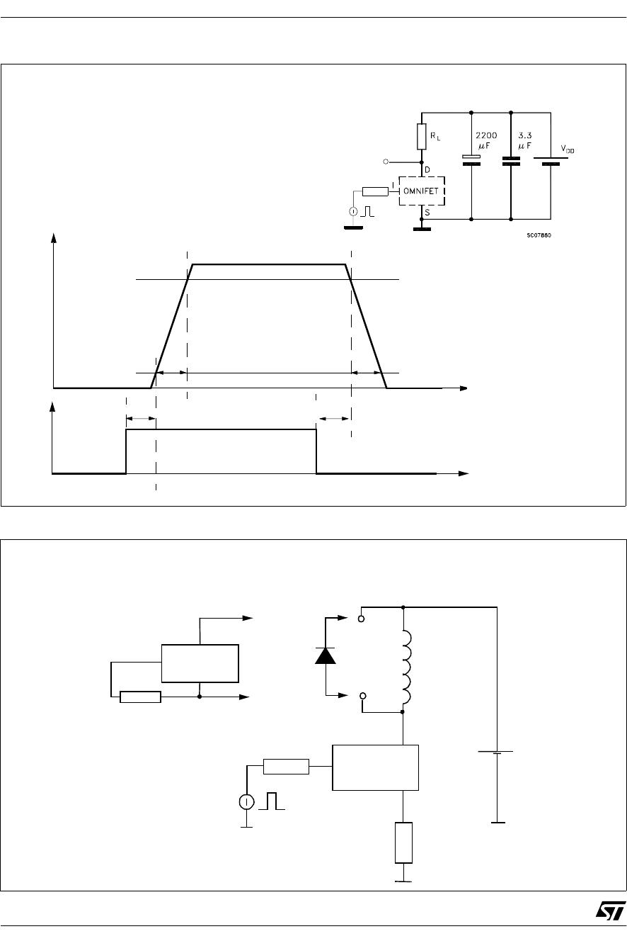
MOSFET and can be used as a switch from DC up
to 25KHz. The only difference from the user’s
standpoint is that a small DC current I
ISS
(typ.
100µA) flows into the INPUT pin in order to supply
the internal circuitry.
The device integrates:
- OVERVOLTAGE CLAMP PROTECTION:
internally set at 45V, along with the rugged
avalanche characteristics of the Power MOSFET
stage give this device unrivalled ruggedness and
energy handling capability. This feature is mainly
important when driving inductive loads.
- LINEAR CURRENT LIMITER CIRCUIT:
limits the drain current I
D
to I
lim
whatever the
INPUT pin voltages is. When the current limiter is
active, the device operates in the linear region, so
power dissipation may exceed the capability of the
heatsink. Both case and junction temperatures
increase, and if this phase lasts long enough,
junction temperature may reach the
overtemperature threshold T
jsh
.
- OVERTEMPERATURE AND SHORT CIRCUIT
PROTECTION:
these are based on sensing the chip temperature
and are not dependent on the input voltage. The
location of the sensing element on the chip in the
power stage area ensures fast, accurate detection
of the junction temperature. Overtemperature
cutout occurs in the range 150 to 190 °C, a typical
value being 170 °C. The device is automatically
restarted when the chip temperature falls of about
15°C below shut-down temperature.
- STATUS FEEDBACK:
in the case of an overtemperature fault condition
(T
j
> T
jsh
), the device tries to sink a diagnostic
current I
gf
through the INPUT pin in order to
indicate fault condition. If driven from a low
impedance source, this current may be used in
order to warn the control circuit of a device
shutdown. If the drive impedance is high enough
so that the INPUT pin driver is not able to supply
the current I
gf
, the INPUT pin will fall to 0V. This
will not however affect the device operation:
no requirement is put on the current capability
of the INPUT pin driver except to be able to
supply the normal operation drive current I
ISS
.
Additional features of this device are ESD
protection according to the Human Body model
and the ability to be driven from a TTL Logic
circuit.