Expand menu
Hello, Sign in
My Account
0
Cart
Home
Products
Sensors
Semiconductors
Passive Components
Connectors
Power
Electromechanical
Optoelectronics
Circuit Protection
Integrated Circuits - ICs
Main Products
Manufacturers
Blog
Services
About OMO
About Us
Contact Us
Check Stock
NLU2G16CMUTCG
P1-P3
P4-P6
P7-P7
NLU2G16
www
.onsemi.com
4
SWITCHING W
A
VEFORMS
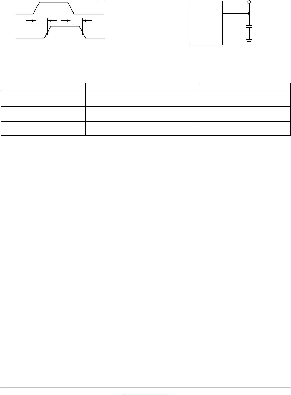
Figure 3. Switching W
aveforms
Y
*Includes all probe and jig capacitance
C
L
*
TEST POINT
DEVICE
UNDER
TEST
OUTPUT
Figure 4. T
est Circuit
50%
50% V
CC
V
CC
GND
t
PLH
t
PHL
A
ORDERING
INFORMA
TION
Device
Package
Shipping
†
NLU2G16MUTCG
UDFN6, 1.2 x 1.0, 0.4P
(Pb−Free)
3000 / T
ape & Reel
NLU2G16AMUTCG
UDFN6, 1.45 x 1.0, 0.5P
(Pb−Free)
3000 / T
ape & Reel
NLU2G16CMUTCG
UDFN6, 1.0 x 1.0, 0.35P
(Pb−Free)
3000 / T
ape & Reel
†
For information on tape and reel specifications, including part orientation and tape sizes, please refer to our T
ape and Reel
Packaging
Specifications Brochure, BRD801
1/D.
NLU2G16
www
.onsemi.com
5
P
ACKAGE
DIMENSIONS
UDFN6 1.0x1.0, 0.35P
CASE 517BX
ISSUE O
NOTES:
1.
DIMENSIONING AND TOLERANCING PER
ASME Y14.5M, 1994.
2.
CONTROLLING DIMENSION: MILLIMETERS.
3.
DIMENSION b APPLIES TO PLA
TED
TERMINAL AND IS MEASURED BETWEEN
0.15 AND 0.20 MM FROM TERMINAL TIP
.
4.
P
ACKAGE DIMENSIONS EXCLUSIVE OF
BURRS AND MOLD FLASH.
*For
additional information on our Pb−Free strategy and soldering
details, please download the
ON Semiconductor Soldering and
Mounting T
echniques Reference Manual, SOLDERRM/D.
SOLDERING FOOTPRINT*
RECOMMENDED
DIM
MIN
MAX
MILLIMETERS
A
0.45
0.55
A1
0.00
0.05
A3
0.13 REF
b
0.12
0.22
D
1.00 BSC
E
1.00 BSC
e
0.35 BSC
L
0.25
0.35
L1
0.30
0.40
A
B
E
D
0.10
C
PIN ONE
REFERENCE
TOP
VIEW
0.10
C
A
A1
0.05
C
0.05
C
C
SEA
TING
PLANE
SIDE VIEW
2X
2X
A3
BOTTOM VIEW
b
e
6X
0.10
B
0.05
A
C
C
L
5X
NOTE 3
L1
1
3
4
6
M
M
DIMENSIONS: MILLIMETERS
0.22
5X
0.48
6X
1.18
0.53
PITCH
0.35
1
PKG
OUTLINE
NLU2G16
www
.onsemi.com
6
P
ACKAGE
DIMENSIONS
UDFN6, 1.2x1.0, 0.4P
CASE 517AA
ISSUE C
NOTES:
1.
DIMENSIONING AND TOLERANCING PER
ASME Y14.5M, 1994.
2.
CONTROLLING DIMENSION: MILLIMETERS.
3.
DIMENSION b APPLIES TO PLA
TED TERMINAL
AND IS MEASURED BETWEEN 0.25 AND
0.30 mm FROM TERMINAL.
4.
COPLANARITY APPLIES TO THE EXPOSED
P
AD AS WELL AS THE TERMINALS.
A
B
E
D
BOTTOM VIEW
b
e
6X
0.10
B
0.05
A
C
C
L
5X
NOTE 3
2X
0.10
C
PIN ONE
REFERENCE
TOP
VIEW
2X
0.10
C
10X
A
A1
(A3)
0.08
C
0.10
C
C
SEA
TING
PLANE
SIDE VIEW
L2
1
3
4
6
DIM
MIN
MAX
MILLIMETERS
A
0.45
0.55
A1
0.00
0.05
A3
0.127 REF
b
0.15
0.25
D
1.20 BSC
E
1.00 BSC
e
0.40 BSC
L
0.30
0.40
L1
0.00
0.15
L1
DET
AIL A
Bottom View
(Optional)
A1
A3
DET
AIL B
Side View
(Optional)
EDGE OF P
ACKAGE
MOLD CMPD
EXPOSED Cu
L2
0.40
0.50
MOUNTING FOOTPRINT*
DIMENSIONS: MILLIMETERS
0.22
6X
0.42
6X
1.07
0.40
PITCH
*For
additional information on our Pb−Free strategy and soldering
details, please download the
ON Semiconductor Soldering and
Mounting T
echniques Reference Manual, SOLDERRM/D.
P1-P3
P4-P6
P7-P7
NLU2G16CMUTCG
Mfr. #:
Buy NLU2G16CMUTCG
Manufacturer:
ON Semiconductor
Description:
Buffers & Line Drivers DUAL BUFFER
Lifecycle:
New from this manufacturer.
Delivery:
DHL
FedEx
Ups
TNT
EMS
Payment:
T/T
Paypal
Visa
MoneyGram
Western
Union
Products related to this Datasheet
NLU2G16CMUTCG
NLU2G16MUTCG
NLU2G16AMX1TCG
NLU2G16CMX1TCG
NLU2G16BMX1TCG
NLU2G16AMUTCG