IRF4905STRLPBF

IRF4905S/L
www.irf.com 7
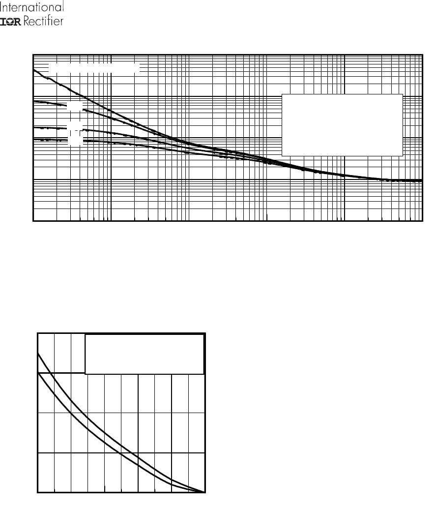
Fig 15. Typical Avalanche Current Vs.Pulsewidth
Fig 16. Maximum Avalanche Energy
Vs. Temperature
Notes on Repetitive Avalanche Curves , Figures 15, 16:
(For further info, see AN-1005 at www.irf.com)
1. Avalanche failures assumption:
Purely a thermal phenomenon and failure occurs at a
temperature far in excess of T
jmax
. This is validated for
every part type.
2. Safe operation in Avalanche is allowed as long asT
jmax
is
not exceeded.
3. Equation below based on circuit and waveforms shown in
Figures 12a, 12b.
4. P
D (ave)
= Average power dissipation per single
avalanche pulse.
5. BV = Rated breakdown voltage (1.3 factor accounts for
voltage increase during avalanche).
6. I
av
= Allowable avalanche current.
7. T = Allowable rise in junction temperature, not to exceed
T
jmax
(assumed as 25°C in Figure 15, 16).
t
av =
Average time in avalanche.
D = Duty cycle in avalanche = t
av
·f
Z
thJC
(D, t
av
) = Transient thermal resistance, see figure 11)
P
D (ave)
= 1/2 ( 1.3·BV·I
av
) = DT/ Z
thJC
I
av
=
2DT/ [1.3·BV·Z
th
]
E
AS (AR)
= P
D (ave)
·t
av
1.0E-06 1.0E-05 1.0E-04 1.0E-03 1.0E-02 1.0E-01
tav (sec)
0.1
1
10
100
1000
A
v
a
l
a
n
c
h
e
C
u
r
r
e
n
t
(
A
)
0.05
Duty Cycle = Single Pulse
0.10
Allowed avalanche Current vs
avalanche pulsewidth, tav
assuming
Tj = 25°C due to
avalanche losses. Note: In no
case should Tj be allowed to
exceed Tjmax
0.01
25 50 75 100 125 150
Starting T
J
, Junction Temperature (°C)
0
40
80
120
160
E
A
R
,
A
v
a
l
a
n
c
h
e
E
n
e
r
g
y
(
m
J
)
TOP Single Pulse
BOTTOM 1% Duty Cycle
I
D
= -42A
IRF4905S/L
8 www.irf.com
Fig 17. Peak Diode Recovery dv/dt Test Circuit for P-Channel
HEXFET
®
Power MOSFETs
Circuit Layout Considerations
Low Stray Inductance
Ground Plane
Low Leakage Inductance
Current Transformer
P.W.
Period
di/dt
Diode Recovery
dv/dt
Ripple 5%
Body Diode Forward Drop
Re-Applied
Voltage
Reverse
Recovery
Current
Body Diode Forward
Current
V
GS
=10V
V
DD
I
SD
Driver Gate Drive
D.U.T. I
SD
Waveform
D.U.T. V
DS
Waveform
Inductor Curent
D =
P. W .
Period
* V
GS
= 5V for Logic Level Devices
*
+
-
+
+
+
-
-
-
R
G
V
DD
dv/dt controlled by R
G
Driver same type as D.U.T.
I
SD
controlled by Duty Factor "D"
D.U.T. - Device Under Test
D.U.T**
Fig 18a. Switching Time Test Circuit
Fig 18b. Switching Time Waveforms
V
DS
90%
10%
V
GS
t
d(on)
t
r
t
d(off)
t
f
V
DS
V
GS
Pulse Width 1 µs
Duty Factor ≤ 0.1 %
R
D
V
GS
V
DD
R
G
D.U.T.
+
-
** Reverse Polarity of D.U.T for P-Channel
IRF4905S/L
www.irf.com 9
D
2
Pak Part Marking Information
D
2
Pak Package Outline (Dimensions are shown in millimeters (inches))
RECTIFIER
INTERNATIONAL
LOGO
LOT CODE
ASSEMBLY
YEAR 0 = 2000
DAT E CODE
PART NUMBER
F530S
A = ASSEMBLY SITE CODE
WEEK 02
P = DE S I GN AT E S L E AD- F R E E
PRODUCT (OPTIONAL)
INTERNAT IONAL
LOT CODE
ASSEMBLY
pos ition indicates "L ead-F ree"
AS S EMBLED ON WW 02, 2000
Note: "P" in as s embly line
IN THE ASSEMBLY LINE "L"
LOT CODE 8024
T HIS IS AN IRF530S WIT H
RECT IFIER
LOGO
LINE L
WEEK 02
YEAR 0 = 2000
DAT E CODE
PART NUMBER
F530S
OR

IRF4905STRLPBF

Mfr. #:
Manufacturer:
Infineon Technologies
Description:
MOSFET MOSFT PCh -55V -74A 20mOhm 120nC
Lifecycle:
New from this manufacturer.
Delivery:
DHL FedEx Ups TNT EMS
Payment:
T/T Paypal Visa MoneyGram Western Union

Products related to this Datasheet