BD63843EFV-E2

Technical Note
4/8
BD63843EFV, BD63847EFV
www.rohm.com
2012.02 - Rev.
A
© 2012 ROHM Co., Ltd. All rights reserved.
Points to notice for terminal description
CLK/Clock input terminal for advancing the electrical angle
CLK is reflected at rising edge. The Electrical angle advances by one for each CLK input.Motor’s misstep will occur if
noise is picked up at the CLK terminal, so please design the pattern in such a way that there is no noise plunging.
MODE0,MODE1/Motor excitation mode setting terminal
Set the step mode.
MODE0 MODE1 Step mode
L L Full step
H L Half step
L H 1/8 step
H H 1/16 step
CW_CCW /Motor rotating direction setting terminal
Set the motor’s rotating direction. Change in setting is reflected at the CLK rising edge immediately after the change in
setting
CW_CCW Rotating direction
L Clockwise (CH2’s current is outputted with a phase lag of 90°in regard to CH1’s current)
H Counter Clockwise(CH2’s current is outputted with a phase lead of 90°in regard to CH1’s current)
ENABLE/Output enable terminal
Turn off forcibly all the output transistors (motor output is open).
At ENABLE=L, electrical angle or operating mode is maintained even if CLK is inputted.
If step modes are changed during ENABLE=L, new step mode is carried out at ENABLE=L to H
ENABLE Motor output
L OPEN (electrical angle maintained)
H ACTIVE
PS/Power save terminal
PS can make circuit standby state and make motor output OPEN. In standby state, translator circuit is reset (initialized)
and electrical angle is initialized.
Please be careful because there is a delay of 40µs(max.) before it is returned from standby state to normal state and the
motor output becomes ACTIVE
PS State
L Standby state (RESET)
H ACTIVE
The electrical angle (initial electrical angle) of each step mode immediately after RESET is as follows
Step mode Initial electrical angle
Full step 45°
Half step 45°
1/8 step
45°
1/16 step 45°
Protection Circuits
Thermal Shutdown (TSD)
This IC has a built-in thermal shutdown circuit for thermal protection. When the IC’s chip temperature rises above 175°C
(Typ.), the motor output becomes OPEN. Also, when the temperature returns to under 150°C (Typ.), it automatically returns
to normal operation. However, even when TSD is in operation, if heat is continued to be added externally, heat overdrive
can lead to destruction.
Over Current Protection (OCP)
This IC has a built in over current protection circuit as a provision against destruction when the motor outputs are shorted
each other or VCC-motor output or motor output-GND is shorted. This circuit latches the motor output to OPEN condition
when the regulated threshold current flows for 4µs (Typ.). It returns with power reactivation or a reset of the PS terminal.
The over current protection circuit’s only aim is to prevent the destruction of the IC from irregular situations such as motor
output shorts, and is not meant to be used as protection or security for the set. Therefore, sets should not be designed to
take into account this circuit’s functions. After OCP operating, if irregular situations continues and the return by power
reactivation or a reset of the PS terminal is carried out repeatly, then OCP operates repeatly and the IC may generate heat
or otherwise deteriorate. When the L value of the wiring is great due to the wiring being long, after the over current has
flowed and the output terminal voltage jumps up and the absolute maximum values may be exceeded and as a result, there
is a possibility of destruction. Also, when current which is over the output current rating and under the OCP detection
current flows, the IC can heat up to over Tjmax=150°C and can deteriorate, so current which exceeds the output rating
should not be applied.
Technical Note
5/8
BD63843EFV, BD63847EFV
www.rohm.com
2012.02 - Rev.
A
© 2012 ROHM Co., Ltd. All rights reserved.
Under Voltage Lock Out (UVLO)
This IC has a built-in under voltage lock out function to prevent false operation such as IC output during power supply under
voltage. When the applied voltage to the VCC terminal goes under 15V (Typ.), the motor output is set to OPEN. This
switching voltage has a 1V (Typ.) hysteresis to prevent false operation by noise etc. Please be aware that this circuit does
not operate during power save mode. Also, the electrical angle is reset when the UVLO circuit operates during CLK-IN drive
mode.
Over Voltage Lock Out (OVLO)
This IC has a built-in over voltage lock out function to protect the IC output and the motor during power supply over voltage.
When the applied voltage to the VCC terminal goes over 32V (Typ.), the motor output is set to OPEN. This switching
voltage has a 1V (Typ.) hysteresis and a 4µs (Typ.) mask time to prevent false operation by noise etc. Although this over
voltage locked out circuit is built-in, there is a possibility of destruction if the absolute maximum value for power supply
voltage is exceeded, therefore the absolute maximum value should not be exceeded. Please be aware that this circuit does
not operate during power save mode.
Ghost Supply Prevention (protects against malfunction when power supply is disconnected)
If a signal (logic input, VREF, MTH) is input when there is no power supplied to this IC, there is a function which prevents
the false operation by voltage supplied via the electrostatic destruction prevention diode from these input terminals to the
VCC to this IC or to another IC’s power supply. Therefore, there is no malfunction of the circuit even when voltage is
supplied to these input terminals while there is no power supply.
Thermal derating curve
HTSSOP-B28 has exposed metal on the back, and it is possible to dissipate heat from a through hole in the back. Also, the
back of board as well as the surfaces has large areas of copper foil heat dissipation patterns, greatly increasing power
dissipation. The back metal is shorted with the back side of the IC chip, being a GND potential, therefore there is a
possibility for malfunction if it is shorted with any potential other than GND, which should be avoided. Also, it is
recommended that the back metal is soldered onto the GND to short. Please note that it has been assumed that this
product will be used in the condition of this back metal performed heat dissipation treatment for increasing heat dissipation
efficiency.
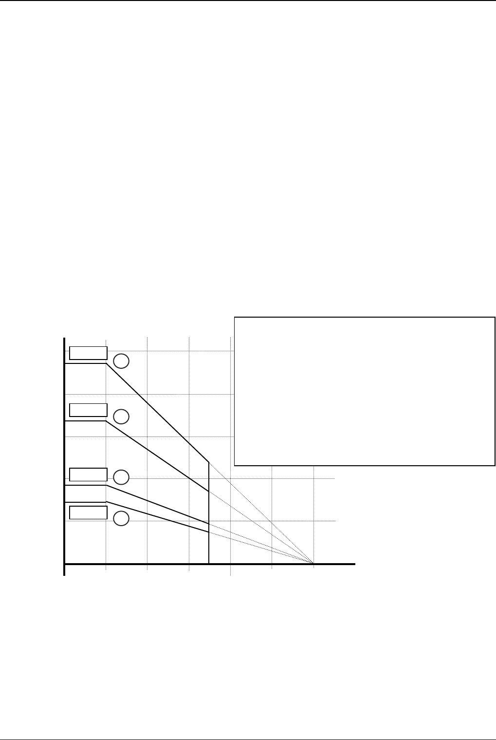
Fig.2 HTSSOP-B28 Thermal derating curve
Ambient temperature:Ta[C]
Power DissipationPd[W]
1.0
100 125
0
4.70W
4
3.30W
3
1.85W
2
1.45W
1
2.0
3.0
4.0
5.0
Measurement machineTH156Kuwano Electric
Measurement conditionROHM board
Board size70mm*70mm*1.6mm
(With through holes on the board)
The exposed metal of the backside is connected to the board with solder.
Board①:1-layer board (Copper foil on the back 0mm)
Board②:2-layer board (Copper foil on the back 15mm*15mm)
Board③:2-layer board (Copper foil on the back 70mm*70mm)
Board④:4-layer board (Copper foil on the back 70mm*70mm)
Board①:θ
ja
=86.2°C W
Board②:θ
ja
=67.6°C W
Board③:θ
ja
=37.9°C W
Board④:θ
ja
=26.6°C W
50 25 85 75 150
Technical Note
6/8
BD63843EFV, BD63847EFV
www.rohm.com
2012.02 - Rev.
A
© 2012 ROHM Co., Ltd. All rights reserved.
Usage Notes
(1) Absolute maximum ratings
An excess in the absolute maximum ratings, such as supply voltage, temperature range of operating conditions, etc., can
break down the devices, thus making impossible to identify breaking mode, such as a short circuit or an open circuit. If
any over rated values will expect to exceed the absolute maximum ratings, consider adding circuit protection devices,
such as fuses.
(2) Connecting the power supply connector backward
Connecting of the power supply in reverse polarity can damage IC. Take precautions when connecting the power supply
lines. An external direction diode can be added.
(3) Power supply Lines
As return of current regenerated by back EMF of FET output happens, take steps such as putting capacitor between
power supply and GND as an electric pathway for the regenerated current. Be sure that there is no problem with each
property such as emptied capacity at lower temperature regarding electrolytic capacitor to decide capacity value. If the
connected power supply does not have sufficient current absorption capacity, regenerative current will cause the voltage
on the power supply line to rise, which combined with the product and its peripheral circuitry may exceed the absolute
maximum ratings. It is recommended to implement a physical safety measure such as the insertion of a voltage clamp
diode between the power supply and GND pins.
(4) GND Potential
The potential of GND pin must be minimum potential in all operating conditions.
(5) Metal on the backside (Define the side where product markings are printed as front)
The metal on the backside is shorted with the backside of IC chip therefore it should be connected to GND. Be aware that
there is a possibility of malfunction or destruction if it is shorted with any potential other than GND.
(6) Thermal design
Use a thermal design that allows for a sufficient margin in light of the power dissipation (Pd) in actual operating conditions.
This IC exposes the metal on the backside of package. Note that this part is assumed to use after providing heat
dissipation treatment to improve heat dissipation efficiency. Try to occupy as wide as possible with heat dissipation
pattern not only on the board surface but also the backside.
(7) Inter-pin shorts and mounting errors
When attaching to a printed circuit board, pay close attention to the direction of the IC and displacement. Improper
attachment may lead to destruction of the IC. There is also possibility of destruction from short circuits which can be
caused by foreign matter entering between outputs or an output and the power supply or GND.
(8) Operation in a strong electric field
Use caution when using the IC in the presence of a strong electromagnetic field as doing so may cause the IC to
malfunction.
(9) ASO
When using the IC, set the output transistor so that it does not exceed absolute maximum ratings or ASO.
(10) Thermal shutdown circuit
The IC has a built-in thermal shutdown circuit (TSD circuit). If the chip temperature becomes Tjmax=150°C, and higher,
coil output to the motor will be open. The TSD circuit is designed only to shut the IC off to prevent runaway thermal
operation. It is not designed to protect or indemnify peripheral equipment. Do not use the TSD function to protect
peripheral equipment.
TSD on temperature [°C] (Typ.) Hysteresis temperature [°C] (Typ.)
175 25
(11) Inspection of the application board
During inspection of the application board, if a capacitor is connected to a pin with low impedance there is a possibility
that it could cause stress to the IC, therefore an electrical discharge should be performed after each process. Also, as a
measure again electrostatic discharge, it should be earthed during the assembly process and special care should be
taken during transport or storage. Furthermore, when connecting to the jig during the inspection process, the power
supply should first be turned off and then removed before the inspection.

BD63843EFV-E2

Mfr. #:
Manufacturer:
Description:
Motor / Motion / Ignition Controllers & Drivers 36V 1A Stepping Motor Driver
Lifecycle:
New from this manufacturer.
Delivery:
DHL FedEx Ups TNT EMS
Payment:
T/T Paypal Visa MoneyGram Western Union

Products related to this Datasheet